ChipApex | Global Electronic Components Supplier
SEARCH
Search Product
Search Post
— IC芯片 | 连接器 | 传感器 | 被动器件 —
Search productSearch post
— IC芯片 | 连接器 | 传感器 | 被动器件 —
Consult the customer manager about the wholesale price.
consultation hotline:86-132-6715-2157
email:[email protected]
Contact the product manager for consultation. One-stop consultation is available.
Do you want a lower wholesale price? Please send us your inquiry and we will reply immediately.
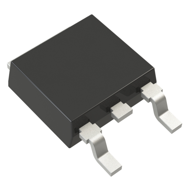
The FCD600N65S3R0 is a single N-channel power MOSFET from the SUPERFET III family, utilizing charge balance technology for low on-resistance and gate charge. It features a 650V drain-source voltage rating with a typical RDS(on) of 493 mΩ at 10V VGS. The device supports a continuous drain current of 6A and has a typical gate charge (Qg) of 11 nC. It operates within a junction temperature range of -55°C to +150°C and is housed in a DPAK-3 (TO-252-3) surface-mount package.
Verify the specific datasheet revision and ordering suffix when sourcing. Confirm that the component meets RoHS compliance and halogen-free requirements as specified by ON Semiconductor. Ensure the supplier provides valid traceability documentation for quality assurance purposes.
Select this component for designs requiring efficient high-voltage switching with minimal drive power. The low gate charge reduces driver complexity, while the super-junction structure offers improved efficiency compared to standard planar technologies in similar voltage classes.
This part belongs to the SUPERFET III series, representing ON Semiconductor's high-voltage super-junction MOSFET family. The series integrates advanced charge balance technology to deliver superior performance metrics relative to previous generations, targeting modern high-density power conversion needs.
Direct substitutes include other SUPERFET III devices with comparable voltage and resistance ratings, such as the FCP600N65S3R0 or FCPF600N65S3R0L-F154, provided pinout compatibility and thermal characteristics are verified against the original design constraints.
The FCD600N65S3R0 has a rated drain-source voltage (VDSS) of 650V.
Yes, the datasheet specifies that these devices are 100% avalanche tested to ensure reliability under transient conditions.
 FCD600N65S3R0
The activity of extra discounts on wholesale prices is in full swing…
Please fill in your contact information and we will send you the latest wholesale price list.