 ChipApex | Global Electronic Components Supplier
SEARCH
Search Product
Search Post
— IC芯片 | 连接器 | 传感器 | 被动器件 —
Search productSearch post
— IC芯片 | 连接器 | 传感器 | 被动器件 —
Consult the customer manager about the wholesale price.
consultation hotline:86-132-6715-2157
email:[email protected]
Contact the product manager for consultation. One-stop consultation is available.
Do you want a lower wholesale price? Please send us your inquiry and we will reply immediately.
The onsemi FCP125N65S3 is an N-channel enhancement-mode MOSFET belonging to the SUPERFET III series, utilizing charge balance technology for high-voltage performance. It features a maximum drain-source voltage (Vdss) of 650 V and a continuous drain current (Id) of 24 A at 25°C. The device exhibits a typical on-resistance (Rds(on)) of 105 mΩ and a gate charge (Qg) of 46 nC. Packaged in a TO-220 through-hole housing with three pins, it supports a maximum power dissipation of 181 W and operates within a temperature range of -55°C to +150°C.
Verify the specific suffix against official datasheets to confirm package variations or tape-and-reel configurations. Confirm RoHS compliance status and environmental declarations directly from the manufacturer's documentation prior to integration. Ensure thermal management designs align with the specified power dissipation limits.
Select this component for high-efficiency hard-switching applications requiring 650 V blocking capability. The low gate charge facilitates faster switching speeds and reduces driver losses. Evaluate thermal resistance requirements carefully given the TO-220 package constraints for high-current operations.
This part belongs to the SUPERFET III family of high-voltage superjunction MOSFETs from onsemi. The series integrates advanced silicon processes to optimize the trade-off between conduction and switching losses, targeting high-frequency power conversion architectures.
Direct substitutes include FCP190N65S3 and FCPF250N65S3L1-F154 within the same product line. Verify pinout compatibility and electrical parameter margins before substitution.
Yes, the SuperFET III technology enables the device to withstand high dv/dt rates while maintaining stable operation.
The typical gate charge (Qg) is 46 nC, which contributes to lower drive power requirements.
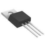 FCP125N65S3
The activity of extra discounts on wholesale prices is in full swing…
Please fill in your contact information and we will send you the latest wholesale price list.





