ChipApex | Global Electronic Components Supplier
SEARCH
Search Product
Search Post
— IC芯片 | 连接器 | 传感器 | 被动器件 —
Search productSearch post
— IC芯片 | 连接器 | 传感器 | 被动器件 —
Consult the customer manager about the wholesale price.
consultation hotline:86-132-6715-2157
email:[email protected]
Contact the product manager for consultation. One-stop consultation is available.
Do you want a lower wholesale price? Please send us your inquiry and we will reply immediately.
The FCU360N65S3R0 is an N-channel power MOSFET from the SUPERFET III series, manufactured by onsemi. It features a 650V drain-source voltage rating and a maximum continuous drain current of 10A at case temperature of 25°C. The device exhibits a maximum on-resistance (RDS(on)) of 360mΩ. Key electrical characteristics include a typical gate charge of 17.5nC and a maximum power dissipation of 83W at 25°C. It operates within a junction temperature range of -55°C to +150°C and supports a single pulse avalanche energy of 40mJ.
Verify the specific suffix R0 against official datasheets to confirm package type and tape/reel specifications. Confirm RoHS compliance status and lead times directly with authorized distributors. Ensure storage conditions adhere to moisture sensitivity levels defined in the manufacturing documentation to prevent damage prior to assembly.
Select this component for designs prioritizing low switching losses and high ruggedness. The SUPERFET III architecture offers optimized performance for hard-switching applications. Evaluate thermal management requirements based on the 83W dissipation rating and ensure adequate heatsinking for sustained operation above 25°C case temperature.
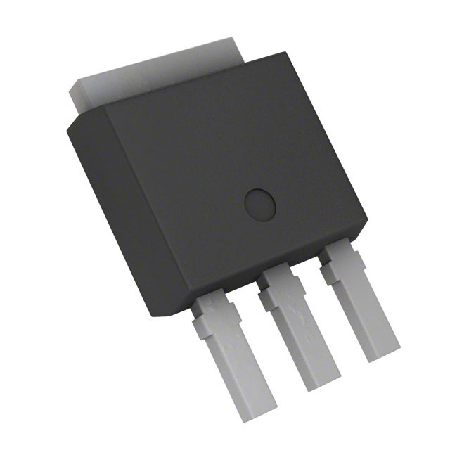
This part belongs to onsemi's SUPERFET III family, which integrates advanced trench gate and field plate technologies. The series is engineered for high-voltage power switching applications, balancing low on-resistance with fast switching speeds. The IPAK package provides a cost-effective solution for through-hole mounting in various power electronic circuits.
Cross-reference with FCP360N65S3R0 for surface-mount TO-252 alternatives or NVD360N65S3 for similar performance in different packages. Verify pinout compatibility and thermal resistance values before substitution to ensure circuit integrity.
Yes, the device is AEC-Q101 qualified and具备 production part approval program (PPAP) capability, making it suitable for automotive electronics.
It utilizes charge balance technology to minimize gate charge and output capacitance, thereby reducing switching losses.
 FCU360N65S3R0
The activity of extra discounts on wholesale prices is in full swing…
Please fill in your contact information and we will send you the latest wholesale price list.