 ChipApex | Global Electronic Components Supplier

SEARCH
Search Product
Search Post
— IC芯片 | 连接器 | 传感器 | 被动器件 —
Search productSearch post
— IC芯片 | 连接器 | 传感器 | 被动器件 —
Consult the customer manager about the wholesale price.
consultation hotline:86-132-6715-2157
email:[email protected]
Contact the product manager for consultation. One-stop consultation is available.
Do you want a lower wholesale price? Please send us your inquiry and we will reply immediately.
FDC6301N is listed in the FET, MOSFET Arrays range at ChipApex. The manufacturer field lists onsemi. Its product description is MOSFET 2N-CH 25V 0.22A SSOT6. Review the specifications below when checking this part for your BOM.
The onsemi FDC6301N is a dual N-channel digital MOSFET housed in an SOT-23-6 package. It integrates two enhancement-mode field-effect transistors with built-in gate-source Zener diodes for ESD protection, rated at over 6kV Human Body Model. Key electrical parameters include a drain-source breakdown voltage (VDS) of 25 V and a continuous drain current (ID) of 220 mA. The device exhibits a maximum on-state resistance (RDS(on)) of 4 Ω at VGS = 4.5 V and 5 Ω at VGS = 2.7 V. The gate-source threshold voltage (VGS(th)) is less than 1.5 V, enabling direct operation in 3 V logic circuits. Operating temperature ranges from -55 °C to +150 °C, with a power dissipation of 300 mW.
Verify component authenticity through authorized distribution channels. Confirm RoHS compliance status via official manufacturer documentation. Check for obsolescence notices as this part may be discontinued or superseded by newer equivalents. Ensure storage conditions meet specified limits to prevent moisture sensitivity issues prior to assembly.
Select this component for space-constrained designs needing dual N-channel switching without external bias networks. Verify that the 220 mA continuous current rating meets load requirements. Ensure the 25 V voltage rating exceeds peak circuit voltages. Consider the 4 Ω RDS(on) for power loss calculations in low-current applications.
This device belongs to the family of digital FETs produced using high cell density DMOS technology. It serves as a compact replacement for multiple discrete digital transistors and bias resistors. The design minimizes on-state resistance while maintaining robust ESD protection suitable for consumer electronics.
Publicly confirmed substitute part numbers are not available in verified sources. Evaluate equivalent dual N-channel digital FETs in SOT-23-6 packages with matching 25 V/220 mA ratings and integrated ESD protection if sourcing is restricted.
Explore related parts through FETs, MOSFETs, Transistors, Discrete Semiconductor Products, all product categories.
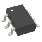 FDC6301N

The activity of extra discounts on wholesale prices is in full swing…
Please fill in your contact information and we will send you the latest wholesale price list.





