 ChipApex | Global Electronic Components Supplier

SEARCH
Search Product
Search Post
— IC芯片 | 连接器 | 传感器 | 被动器件 —
Search productSearch post
— IC芯片 | 连接器 | 传感器 | 被动器件 —
Consult the customer manager about the wholesale price.
consultation hotline:86-132-6715-2157
email:[email protected]
Contact the product manager for consultation. One-stop consultation is available.
Do you want a lower wholesale price? Please send us your inquiry and we will reply immediately.
FDC6304P is listed in the FET, MOSFET Arrays range at ChipApex. The manufacturer field lists onsemi. Its product description is MOSFET 2P-CH 25V 0.46A SSOT6. Review the specifications below when checking this part for your BOM.
The FDC6304P is a P-Channel Enhancement Mode Field Effect Transistor manufactured by onsemi. It utilizes PowerTrench technology to achieve low on-resistance and fast switching speeds. The device features a drain-source voltage rating of 20 V and a continuous drain current capability of 5.5 A at 25°C ambient temperature. Key electrical parameters include a maximum drain-source on-resistance of 45 mΩ at a gate-source voltage of 4.5 V, and a threshold voltage ranging from 0.8 V to 1.5 V. The component is housed in a compact DFN3 package with dimensions of 2 mm by 2.5 mm, designed for surface mount applications.
Verify the manufacturer part number against official onsemi documentation to ensure authenticity. Confirm that the specific ordering suffix matches the required packaging configuration. Check RoHS compliance status and material content declarations as specified in the datasheet. Ensure storage conditions adhere to moisture sensitivity level requirements prior to assembly.
Select this component when a compact P-channel MOSFET with low on-resistance is required for 20 V systems. Evaluate the thermal performance under expected load conditions to ensure junction temperatures remain within safe operating limits. Consider the gate charge characteristics for high-frequency switching applications to minimize driver losses.
This device belongs to the FDC6304 family of PowerTrench P-Channel MOSFETs. It shares similar electrical characteristics with other members of the series but may differ in packaging or specific parameter tolerances. The family is designed for general-purpose power switching applications requiring small form factors.
Publicly confirmed substitute part numbers are not available in the provided reference data. Verify pinout compatibility and electrical specifications before considering alternative components from other manufacturers.
The maximum drain-source voltage (Vdss) is rated at 20 V.
The maximum drain-source on-resistance (Rds(on)) is 45 mΩ when measured at a gate-source voltage of 4.5 V and a drain current of 5.5 A.
The component is supplied in a DFN3 package with dimensions of 2 mm by 2.5 mm.
Explore related parts through FETs, MOSFETs, Transistors, Discrete Semiconductor Products, all product categories.
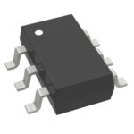 FDC6304P

The activity of extra discounts on wholesale prices is in full swing…
Please fill in your contact information and we will send you the latest wholesale price list.





