 ChipApex | Global Electronic Components Supplier

SEARCH
Search Product
Search Post
— IC芯片 | 连接器 | 传感器 | 被动器件 —
Search productSearch post
— IC芯片 | 连接器 | 传感器 | 被动器件 —
Consult the customer manager about the wholesale price.
consultation hotline:86-132-6715-2157
email:[email protected]
Contact the product manager for consultation. One-stop consultation is available.
Do you want a lower wholesale price? Please send us your inquiry and we will reply immediately.
FDG6302P is listed in the FET, MOSFET Arrays range at ChipApex. The manufacturer field lists onsemi. Its product description is MOSFET 2P-CH 25V 0.14A SC88. Review the specifications below when checking this part for your BOM.
The FDG6302P is a dual P-channel digital FET manufactured by onsemi, housed in an SC70-6 (SOT-363) surface-mount package. It features a drain-source voltage rating of -25 V and a continuous drain current of -0.14 A. The device exhibits a static drain-source on-resistance of 10 Ω at VGS = -4.5 V and 13 Ω at VGS = -2.7 V. Gate threshold voltage ranges from -0.65 V to -1.5 V, enabling direct operation in 3 V circuits. Maximum power dissipation is 0.3 W with a junction-to-ambient thermal resistance of 415 °C/W. Operating temperature spans -55 °C to +150 °C.
Verify the manufacturer origin carefully as this component was originally produced by Fairchild Semiconductor before its acquisition by onsemi. Confirm that the specific revision matches the required datasheet specifications. Ensure the SC70-6 package dimensions align with the target PCB footprint constraints during the procurement phase.
Select this component when a compact dual P-channel solution is required for low current switching tasks. The low gate threshold voltage makes it suitable for battery-powered systems operating at 3 V. Evaluate the thermal resistance requirements against the available copper area on the printed circuit board to ensure adequate heat dissipation under continuous load conditions.
This device belongs to the category of digital FETs designed to replace traditional bipolar junction transistors. It utilizes high cell density DMOS technology to minimize on-state resistance within a small form factor. The product line targets applications demanding efficient space utilization and low voltage compatibility in consumer electronics.
FDG6302P
Yes, the pinout is symmetrical; Pin 1 and Pin 4 are interchangeable without affecting device functionality.
The device has an ESD rating of 6.0 kV according to the MIL-STD-883D Human Body Model standard.
At VGS = -4.5 V and ID = -0.14 A, the RDS(ON) increases from a typical 10 Ω at 25°C to 17 Ω at 125°C.
Explore related parts through FETs, MOSFETs, Transistors, Discrete Semiconductor Products, all product categories.
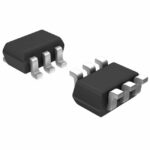 FDG6302P

The activity of extra discounts on wholesale prices is in full swing…
Please fill in your contact information and we will send you the latest wholesale price list.





