 ChipApex | Global Electronic Components Supplier

SEARCH
Search Product
Search Post
— IC芯片 | 连接器 | 传感器 | 被动器件 —
Search productSearch post
— IC芯片 | 连接器 | 传感器 | 被动器件 —
Consult the customer manager about the wholesale price.
consultation hotline:86-132-6715-2157
email:[email protected]
Contact the product manager for consultation. One-stop consultation is available.
Do you want a lower wholesale price? Please send us your inquiry and we will reply immediately.
FDG6313N is listed in the FET, MOSFET Arrays range at ChipApex. The manufacturer field lists onsemi. Its product description is MOSFET 2N-CH 25V 0.5A SC88. Review the specifications below when checking this part for your BOM.
The FDG6313N is a dual N-channel digital FET in an SC70-6 package. It features a Drain-Source Voltage (VDSS) of 25 V and continuous Drain Current (ID) of 0.5 A. The static Drain-Source On-Resistance (RDS(ON)) is 0.45 Ω at VGS=4.5 V and 0.60 Ω at VGS=2.7 V. Gate Threshold Voltage (VGS(th)) ranges from 0.65 V to 1.5 V. Maximum Power Dissipation (PD) is 0.3 W, with a Junction-to-Ambient Thermal Resistance (RθJA) of 415 °C/W. Operating temperature spans -55°C to +150°C.
Verify the manufacturer origin as Fairchild Semiconductor or onsemi, noting that onsemi acquired Fairchild's semiconductor business. Confirm the component status is active or full production rather than obsolete. Ensure the datasheet revision matches the required specifications before procurement.
Select this component when a dual N-channel configuration is required in a minimal footprint. Verify that the 0.5 A continuous current rating meets the load requirements. Check that the 25 V breakdown voltage provides sufficient margin for the application's supply voltage.
This device belongs to the SuperSOT-6 family of dual MOSFETs. It utilizes proprietary high cell density DMOS technology developed by Fairchild Semiconductor. The component is designed specifically for space-constrained portable electronics and low voltage logic interfacing.
Check for equivalents within the FDG series such as FDG6312N or FDG6322C if pinout compatibility differs. Verify RDS(ON) and VDSS ratings against the original design requirements when sourcing substitutes.
Yes, the pinouts are symmetrical; pin 1 and pin 4 are interchangeable without affecting functionality.
The maximum power dissipation is 0.3 W at 25°C ambient temperature.
Yes, the very low level gate drive requirements allow direct operation in 3 V circuits.
Explore related parts through FETs, MOSFETs, Transistors, Discrete Semiconductor Products, all product categories.
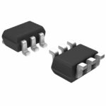 FDG6313N

The activity of extra discounts on wholesale prices is in full swing…
Please fill in your contact information and we will send you the latest wholesale price list.





