ChipApex | Global Electronic Components Supplier

SEARCH
Search Product
Search Post
— IC芯片 | 连接器 | 传感器 | 被动器件 —
Search productSearch post
— IC芯片 | 连接器 | 传感器 | 被动器件 —
Consult the customer manager about the wholesale price.
consultation hotline:86-132-6715-2157
email:[email protected]
Contact the product manager for consultation. One-stop consultation is available.
Do you want a lower wholesale price? Please send us your inquiry and we will reply immediately.
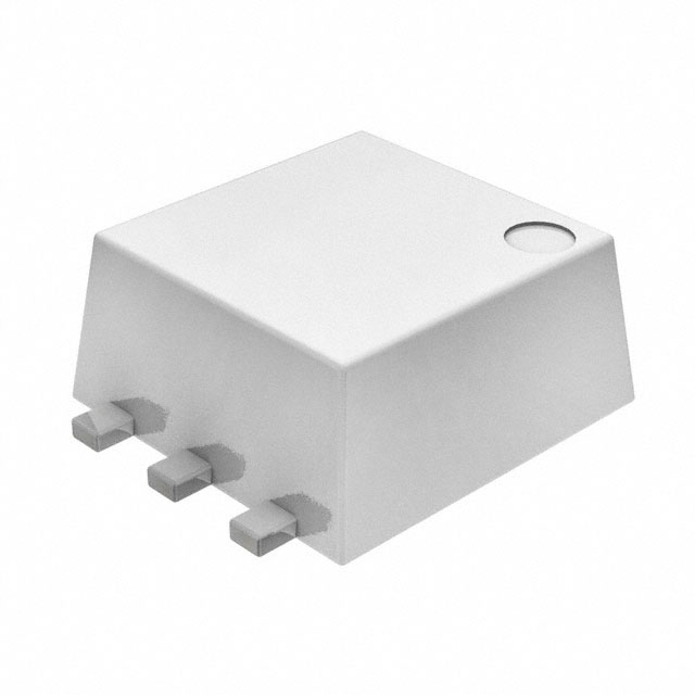
FDJ1032C is listed in the FET, MOSFET Arrays range at ChipApex. The manufacturer field lists onsemi. Its product description is MOSFET N/P-CH 20V 3.2A SC75-6. Review the specifications below when checking this part for your BOM.
The FDJ1032C is a complementary PowerTrench MOSFET pair in an FLMP SC75 package. It integrates a P-Channel device (Q1) rated at -20 V and -2.8 A, and an N-Channel device (Q2) rated at 20 V and 3.2 A. The Q1 exhibits a maximum RDS(ON) of 160 mΩ at VGS = -4.5 V, while the Q2 achieves 90 mΩ at VGS = 4.5 V. Operating junction temperatures range from -55°C to +150°C with thermal resistance values of 80°C/W (junction-to-ambient) and 5°C/3°C (junction-to-case for Q1/Q2).
Verify component authenticity through authorized Fairchild Semiconductor distributors due to counterfeiting risks. Confirm RoHS compliance status and check for obsolete product status notifications before procurement planning. Ensure supply chain traceability meets quality standards.
Select this complementary pair for low-voltage battery-powered applications requiring minimal inline power loss. Evaluate thermal requirements against the 80°C/W junction-to-ambient resistance. Verify that system voltage does not exceed the 20 V drain-source breakdown limits for either channel.
Manufactured by Fairchild Semiconductor using the PowerTrench process, this component represents a specialized solution for integrated power management. The FLMP SC75 packaging allows for compact board layouts while maintaining thermal efficiency suitable for portable electronics and industrial control modules.
No public confirmed substitute part numbers are available in the provided documentation. Cross-referencing requires matching complementary N/P-channel configurations, voltage ratings, and package dimensions.
The N-Channel device (Q2) supports a maximum continuous drain current of 3.2 A at TA = 25°C.
The gate threshold voltage temperature coefficient is +3 mV/°C for the P-Channel (Q1) and -3 mV/°C for the N-Channel (Q2).
The typical total gate charge (Qg) for the P-Channel device (Q1) is 3 nC under test conditions of VDS = -10 V and ID = -2.8 A.
Explore related parts through FETs, MOSFETs, Transistors, Discrete Semiconductor Products, all product categories.
 FDJ1032C

The activity of extra discounts on wholesale prices is in full swing…
Please fill in your contact information and we will send you the latest wholesale price list.