 ChipApex | Global Electronic Components Supplier

SEARCH
Search Product
Search Post
— IC芯片 | 连接器 | 传感器 | 被动器件 —
Search productSearch post
— IC芯片 | 连接器 | 传感器 | 被动器件 —
Consult the customer manager about the wholesale price.
consultation hotline:86-132-6715-2157
email:[email protected]
Contact the product manager for consultation. One-stop consultation is available.
Do you want a lower wholesale price? Please send us your inquiry and we will reply immediately.
FDW2512NZ is listed in the FET, MOSFET Arrays range at ChipApex. The manufacturer field lists onsemi. Its product description is MOSFET 2N-CH 20V 6A 8TSSOP. Review the specifications below when checking this part for your BOM.
The FDW2512NZ is a dual N-Channel PowerTrench MOSFET in a TSSOP-8 package. It features a 20V drain-source voltage rating and an extended gate-source voltage range of ±12V. At VGS = 4.5V, the on-resistance (rDS(ON)) is typically 0.017Ω with a maximum of 0.028Ω at ID = 6.0A. At VGS = 2.5V, rDS(ON) is typically 0.022Ω with a maximum of 0.036Ω at ID = 5.3A. The device supports continuous drain currents up to 6.0A at 25°C case temperature. Total gate charge is 8nC typical at 4.5V. Thermal resistance junction-to-ambient is 77°C/W on a 1-inch copper pad.
Verify the component origin as Fairchild Semiconductor, now part of onsemi, using the provided datasheet revision A1. Confirm the package marking '2512NZ' matches the physical device. Ensure the ordering suffix corresponds to the specified reel size and tape width if purchasing in bulk quantities.
Select this component for portable electronics requiring low on-resistance at low gate drive voltages. Verify that the required continuous drain current does not exceed 6.0A at 25°C or 3.3A at 100°C case temperature. Ensure the circuit operates within the 20V drain-source and ±12V gate-source absolute maximum ratings.
This dual MOSFET belongs to the PowerTrench family, optimized for portable applications. It integrates two independent N-channel devices in a single compact package to save board space. The design prioritizes low conduction losses while maintaining fast switching performance through reduced gate charge characteristics.
No public confirmed substitute part numbers are documented in the source material.
The absolute maximum gate-source voltage is ±12V.
At VGS = 4.5V, rDS(ON) is typically 0.017Ω. At VGS = 2.5V, it increases to typically 0.022Ω.
It is 77°C/W when mounted on a 1-inch square copper pad on FR-4, and 114°C/W on a minimum copper pad.
Explore related parts through FETs, MOSFETs, Transistors, Discrete Semiconductor Products, all product categories.
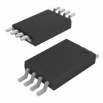 FDW2512NZ

The activity of extra discounts on wholesale prices is in full swing…
Please fill in your contact information and we will send you the latest wholesale price list.





