 ChipApex | Global Electronic Components Supplier

SEARCH
Search Product
Search Post
— IC芯片 | 连接器 | 传感器 | 被动器件 —
Search productSearch post
— IC芯片 | 连接器 | 传感器 | 被动器件 —
Consult the customer manager about the wholesale price.
consultation hotline:86-132-6715-2157
email:[email protected]
Contact the product manager for consultation. One-stop consultation is available.
Do you want a lower wholesale price? Please send us your inquiry and we will reply immediately.
GPI65015DFN is listed in the Single FETs, MOSFETs range at ChipApex. The manufacturer field lists GaNPower. Its product description is GANFET N-CH 650V 15A DFN 8X8. Review the specifications below when checking this part for your BOM.
The GPI65015DFN is an N-channel enhancement-mode Gallium Nitride (GaN) High Electron Mobility Transistor (HEMT) manufactured by GaNPower International Inc. It features a breakdown voltage of 650 V and a maximum drain-source current of 15 A at 25°C case temperature. The device utilizes proprietary E-mode GaN on silicon technology to achieve an ultra-low static drain-source on-resistance of 85 mΩ typical value. Packaged in an 8x8 mm DFN surface-mount configuration with a bottom thermal pad, it exhibits extremely low input capacitance of 116 pF and zero reverse recovery charge.
Verify the specific package dimensions against the official datasheet before PCB layout finalization. Confirm that gate drive circuits are optimized for the required voltage levels and slew rates to handle the high dv/dt characteristics safely. Ensure thermal management solutions account for the junction-to-case thermal resistance specified in the absolute maximum ratings section.
Select this component when designing systems requiring high efficiency and compact form factors due to its low profile packaging. Consider the need for specialized gate drivers capable of handling high transient immunity, as standard silicon MOSFET drivers may not suffice. Evaluate the thermal requirements carefully given the 15 A current rating and the specific thermal resistance values provided for the DFN package.
This device belongs to the family of N-channel 650V GaN Power HEMTs produced by GaNPower International Inc. It represents a solid-state solution leveraging advanced semiconductor materials to replace traditional silicon-based power switches. The product line focuses on delivering high-performance power conversion components for modern electronic systems demanding improved energy efficiency.
Direct pin-to-pin replacement with silicon MOSFETs or IGBTs is not recommended due to differences in gate driving voltage requirements and high dv/dt slew rates. Specialized drivers and optimized PCB layouts are necessary to minimize circuit parasitics when substituting into existing designs.
No, direct replacement is not advised. Due to different gate driving voltage requirements and extremely high dv/dt slew rates, special drivers and optimized PCB layouts are recommended to minimize the impact from circuit parasitics.
No, users do not need to parallel an FRD to suppress body diode reverse recovery effects because GaN HEMTs have no inherent PN junction diodes causing such issues and can operate in both first and third quadrants.
Explore related parts through FETs, MOSFETs, Transistors, Discrete Semiconductor Products, all product categories.
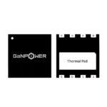 GPI65015DFN

The activity of extra discounts on wholesale prices is in full swing…
Please fill in your contact information and we will send you the latest wholesale price list.





