ChipApex | Global Electronic Components Supplier

SEARCH
Search Product
Search Post
— IC芯片 | 连接器 | 传感器 | 被动器件 —
Search productSearch post
— IC芯片 | 连接器 | 传感器 | 被动器件 —
Consult the customer manager about the wholesale price.
consultation hotline:86-132-6715-2157
email:[email protected]
Contact the product manager for consultation. One-stop consultation is available.
Do you want a lower wholesale price? Please send us your inquiry and we will reply immediately.
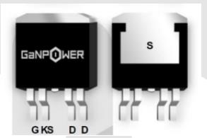
GPI65030TO5L is listed in the Single FETs, MOSFETs range at ChipApex. The manufacturer field lists GaNPower. Its product description is GaNFET N-CH 650V 30A TO263-5L. Review the specifications below when checking this part for your BOM.
The GPI65030TO5L is an N-channel enhancement-mode GaN Power HEMT in a TO263-5L package. It features a 650 V drain-source breakdown voltage and a typical static on-resistance of 55 mΩ at 25°C. The device supports a maximum DC drain current of 30 A at 25°C case temperature, reducing to 24 A at 100°C. Key dynamic parameters include a total gate charge of 5.8 nC, input capacitance of 241 pF, and zero reverse recovery charge. It offers a high drain-source voltage slew rate capability of 200 V/ns and operates with a maximum junction temperature of 150°C.
Verify the specific datasheet version (e.g., v1.2) against your design requirements, as electrical characteristics may vary between revisions. Confirm that the TO263-5L package thermal pad connection aligns with your PCB layout strategy, noting that the source terminal is connected to the thermal pad rather than the drain. Ensure your gate driver circuitry can handle the high dv/dt slew rate and provides appropriate negative gate voltage bias if required for robust off-state performance.
Select this component when designing for high power density and efficiency in medium-voltage applications up to 650V. The low gate charge and fast switching speeds make it suitable for high-frequency converters where minimizing switching losses is critical. Consider the thermal management requirements carefully, as the device supports high currents but requires adequate heat sinking to maintain performance within the specified junction temperature limits.
This device belongs to the GaNPower International Inc. portfolio of E-mode GaN HEMTs built on proprietary silicon-based technology. Unlike traditional silicon MOSFETs, these devices leverage the material properties of Gallium Nitride to achieve significantly lower on-resistance and faster switching times. The TO263-5L package provides a cost-effective solution for designers transitioning from silicon to GaN while maintaining compatibility with standard surface-mount assembly processes.
GaN HEMTs are not direct pin-to-pin replacements for silicon MOSFETs or IGBTs due to differences in gate driving voltage requirements and sensitivity to parasitic inductances. Designers must implement optimized PCB layouts and specialized gate drivers to manage the high dv/dt capabilities effectively.
Explore related parts through FETs, MOSFETs, Transistors, Discrete Semiconductor Products, all product categories.
 GPI65030TO5L

The activity of extra discounts on wholesale prices is in full swing…
Please fill in your contact information and we will send you the latest wholesale price list.