ChipApex | Global Electronic Components Supplier

SEARCH
Search Product
Search Post
— IC芯片 | 连接器 | 传感器 | 被动器件 —
Search productSearch post
— IC芯片 | 连接器 | 传感器 | 被动器件 —
Consult the customer manager about the wholesale price.
consultation hotline:86-132-6715-2157
email:[email protected]
Contact the product manager for consultation. One-stop consultation is available.
Do you want a lower wholesale price? Please send us your inquiry and we will reply immediately.
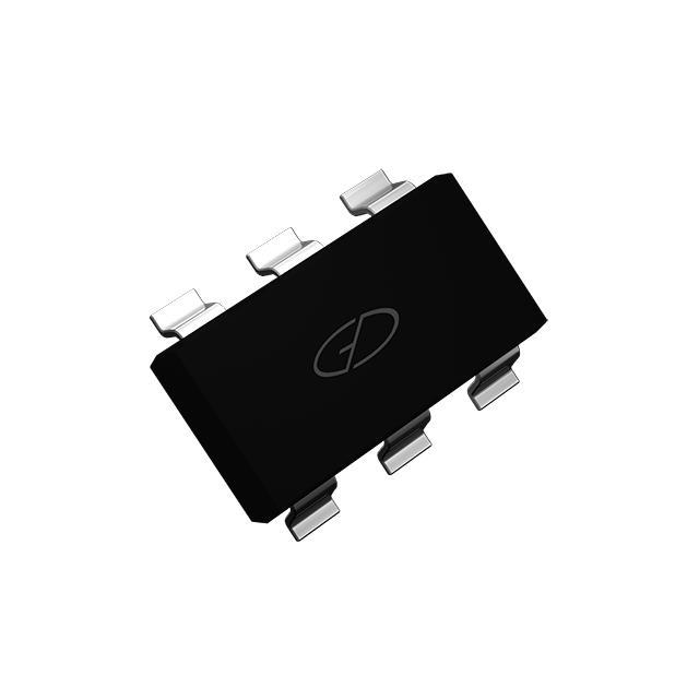
GSFK0300 is listed in the FET, MOSFET Arrays range at ChipApex. The manufacturer field lists Good-Ark Semiconductor. Its product description is MOSFET 2N-CH 30V 0.8A SOT363. Review the specifications below when checking this part for your BOM.
The GSFK0300 is a dual N-channel MOSFET manufactured by Good-Ark Semiconductor, housed in an SOT-363 surface-mount package. It features a drain-source voltage (VDS) of 30V and a continuous drain current (ID) of 800mA at 25°C case temperature. The device exhibits a maximum on-resistance (RDS(on)) of 450mΩ at VGS=4.5V and ID=0.3A, or 650mΩ at VGS=2.5V and ID=0.2A. Gate threshold voltage ranges from 0.5V to 1.2V. Total gate charge is typically 2.6nC with a maximum of 5.2nC at VGS=4.5V. Operating junction temperature spans -55°C to +150°C.
Verify the specific ordering suffix against the manufacturer's official documentation to ensure correct carrier quantity and RoHS compliance status. Confirm that the SOT-363 package marking code matches the required identification standards for your assembly process. Ensure thermal management strategies account for the specified junction-to-ambient thermal resistance when designing for ambient temperatures above 25°C.
Select this component for applications requiring dual N-channel isolation in a minimal footprint. The low gate charge supports high-frequency operation, while the 30V rating provides adequate headroom for low-voltage systems. Consider the RDS(on) increase at lower gate drive voltages if using 2.5V logic levels. Verify that the pulsed drain current capability meets transient load requirements without exceeding thermal limits.
This device belongs to Good-Ark Semiconductor's discrete semiconductor product line, specifically categorized under single and dual FETs. It utilizes silicon metal-oxide semiconductor technology designed for general-purpose switching. The SOT-363 package allows for automated surface-mount assembly, integrating two independent channels into a single component to reduce board space compared to individual packages.
Public confirmed substitute part numbers are not available in the provided documentation. Verify pinout compatibility and electrical parameters such as VDS, ID, and RDS(on) before considering alternative manufacturers' dual MOSFETs in the SOT-363 package.
The absolute maximum gate-source voltage (VGS) is ±12V.
Yes, the datasheet specifies Drain-Source Diode Characteristics, including forward voltage (VSD) and source current ratings, indicating the presence of intrinsic body diodes.
The maximum RDS(on) is 450mΩ at VGS=4.5V and 650mΩ at VGS=2.5V, indicating higher resistance at lower gate drive voltages.
Explore related parts through FETs, MOSFETs, Transistors, Discrete Semiconductor Products, all product categories.
 GSFK0300

The activity of extra discounts on wholesale prices is in full swing…
Please fill in your contact information and we will send you the latest wholesale price list.