ChipApex | Global Electronic Components Supplier

SEARCH
Search Product
Search Post
— IC芯片 | 连接器 | 传感器 | 被动器件 —
Search productSearch post
— IC芯片 | 连接器 | 传感器 | 被动器件 —
Consult the customer manager about the wholesale price.
consultation hotline:86-132-6715-2157
email:[email protected]
Contact the product manager for consultation. One-stop consultation is available.
Do you want a lower wholesale price? Please send us your inquiry and we will reply immediately.
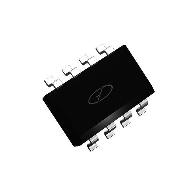
GSFQ4953 is listed in the FET, MOSFET Arrays range at ChipApex. The manufacturer field lists Good-Ark Semiconductor. Its product description is MOSFET 2P-CH 30V 5.4A 8SOP. Review the specifications below when checking this part for your BOM.
The GSFQ4953 is a dual P-channel MOSFET featuring a -30V drain-source voltage (VDS) and a continuous drain current (ID) of -5.4A at steady-state conditions. It exhibits a maximum on-resistance (RDS(ON)) of 58mΩ at VGS=-10V and 85mΩ at VGS=-4.5V. The device supports a pulsed drain current (IDM) of -20A and offers a power dissipation rating of 2W with a junction-to-ambient thermal resistance (RθJA) of 50°C/W. Operating temperatures range from -55°C to +150°C, housed in an SOP-8 package.
Verify the specific ordering suffix against the manufacturer's documentation to confirm packaging details. Confirm that the requested quantity aligns with the standard shipping unit specified in the order information section. Ensure the component marking matches the datasheet requirements for identification purposes during assembly.
Select this component when a dual P-channel configuration is required within a compact SOP-8 footprint. Evaluate the thermal performance based on the 50°C/W junction-to-ambient resistance value for your specific PCB layout. Consider the gate charge specifications for driving requirements in high-frequency switching environments.
This component belongs to the category of dual P-channel enhancement mode MOSFETs designed for power management applications. It integrates two independent P-channel devices into a single package to save board space. The technology focuses on reducing conduction losses through optimized trench cell structures.
Cross-reference electrical parameters such as VDS, ID, and RDS(ON) with alternative dual P-channel MOSFETs in SOP-8 packages. Verify pinout compatibility and thermal characteristics before substitution.
The device supports a pulsed drain current (IDM) of -20A, limited by the maximum junction temperature.
The maximum RDS(ON) is 58mΩ at VGS=-10V and increases to 85mΩ at VGS=-4.5V under specified test conditions.
The operating junction and storage temperature range extends from -55°C to +150°C.
Explore related parts through FETs, MOSFETs, Transistors, Discrete Semiconductor Products, all product categories.
 GSFQ4953

The activity of extra discounts on wholesale prices is in full swing…
Please fill in your contact information and we will send you the latest wholesale price list.