ChipApex | Global Electronic Components Supplier
SEARCH
Search Product
Search Post
— IC芯片 | 连接器 | 传感器 | 被动器件 —
Search productSearch post
— IC芯片 | 连接器 | 传感器 | 被动器件 —
Consult the customer manager about the wholesale price.
consultation hotline:86-132-6715-2157
email:[email protected]
Contact the product manager for consultation. One-stop consultation is available.
Do you want a lower wholesale price? Please send us your inquiry and we will reply immediately.
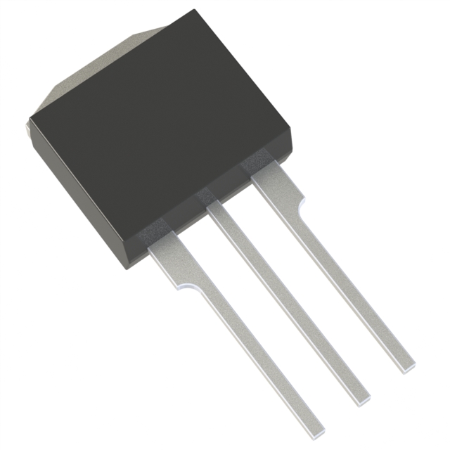
The GT10J312 is a third-generation silicon N-channel IGBT from Toshiba Semiconductor and Storage, designed for high-power switching and motor control applications. It features an enhancement mode structure with an integrated fast recovery diode (FRD) between the emitter and collector. The device supports a collector-emitter voltage of 600 V and a continuous DC collector current of 10 A at 25°C. Key electrical parameters include a maximum saturation voltage of 2.7 V and a maximum fall time of 0.30 μs under specified inductive load conditions.
Verify component authenticity by checking the marking code '10J312' against official Toshiba documentation. Confirm package type availability, as the datasheet lists both JEDEC and JEITA variants with distinct weights. Ensure compliance with RoHS requirements through direct supplier confirmation prior to procurement.
Evaluate thermal management requirements based on a junction-to-case thermal resistance of 2.08 °C/W for the IGBT and 3.76 °C/W for the diode. Design gate drive circuits to accommodate ±15 V swing and ensure peak forward current ratings are not exceeded during transient events. Verify operating temperature limits do not exceed 150°C junction temperature.
This component belongs to Toshiba's insulated gate bipolar transistor lineup targeting industrial power electronics. It represents a specific generation of devices optimized for balancing switching speed and conduction losses. The product line includes variations such as the GT10J312(SM), indicating different packaging or marking standards within the same electrical specification family.
Publicly confirmed substitute part numbers are not available in the provided documentation. Cross-referencing requires matching 600V/10A specifications and TO-220-style packaging constraints.
 GT10J312(Q)
The activity of extra discounts on wholesale prices is in full swing…
Please fill in your contact information and we will send you the latest wholesale price list.