 ChipApex | Global Electronic Components Supplier

SEARCH
Search Product
Search Post
— IC芯片 | 连接器 | 传感器 | 被动器件 —
Search productSearch post
— IC芯片 | 连接器 | 传感器 | 被动器件 —
Consult the customer manager about the wholesale price.
consultation hotline:86-132-6715-2157
email:[email protected]
Contact the product manager for consultation. One-stop consultation is available.
Do you want a lower wholesale price? Please send us your inquiry and we will reply immediately.
HTMN5130SSD-13 is listed in the FET, MOSFET Arrays range at ChipApex. The manufacturer field lists Diodes Incorporated. Its product description is MOSFET 2N-CH 55V 2.6A 8SO. Review the specifications below when checking this part for your BOM.
The HTMN5130SSD-13 is a dual N-channel enhancement mode MOSFET manufactured by Diodes Incorporated. It features a maximum drain-source voltage (V(BR)DSS) of 55 V and operates within a junction temperature range of -55°C to +175°C. The device provides a maximum static drain-source on-resistance (RDS(ON)) of 130 mΩ at VGS = 10 V and 200 mΩ at VGS = 4.5 V. Continuous drain current ratings are 2.86 A at TA = +25°C and 2.3 A at TA = +70°C. Total gate charge is 8.9 nC at VGS = 10 V. The component is housed in an SO-8 surface-mount package.
Verify the specific revision level of the datasheet DS36319 Rev. 4 - 3 when sourcing components. Confirm that the received parts match the marking information provided in the official documentation. Ensure compliance with the specified storage and handling requirements for moisture sensitivity level 1 devices during assembly processes.
Select this component for designs requiring a 55 V dual N-channel MOSFET capable of operating up to 175°C junction temperature. Evaluate thermal resistance parameters against the expected ambient conditions and copper pad layout. Consider the RDS(ON) values at both 10 V and 4.5 V gate drive levels to ensure compatibility with the control circuitry logic levels.
This part belongs to the HTMN series of dual N-channel MOSFETs from Diodes Incorporated. It utilizes an SO-8 case style with molded plastic green molding compound. The device is marked with 'e3' indicating tin finish annealed over a copper leadframe. The document explicitly states this part is not recommended for new design.
The datasheet explicitly states there is no alternate part for the HTMN5130SSD. Designers should consult the manufacturer for updated recommendations or select a different component from the current portfolio suitable for new designs.
The maximum operating and storage junction temperature range is -55°C to +175°C.
Yes, the device is qualified to AEC-Q101 standards for high reliability.
The body diode reverse recovery time (trr) is typically 30.8 ns at IF = 1.5A and dI/dt = 100A/μs.
Explore related parts through FETs, MOSFETs, Transistors, Discrete Semiconductor Products, all product categories.
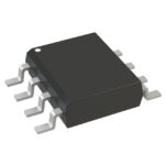 HTMN5130SSD-13

The activity of extra discounts on wholesale prices is in full swing…
Please fill in your contact information and we will send you the latest wholesale price list.





