ChipApex | Global Electronic Components Supplier

SEARCH
Search Product
Search Post
— IC芯片 | 连接器 | 传感器 | 被动器件 —
Search productSearch post
— IC芯片 | 连接器 | 传感器 | 被动器件 —
Consult the customer manager about the wholesale price.
consultation hotline:86-132-6715-2157
email:[email protected]
Contact the product manager for consultation. One-stop consultation is available.
Do you want a lower wholesale price? Please send us your inquiry and we will reply immediately.
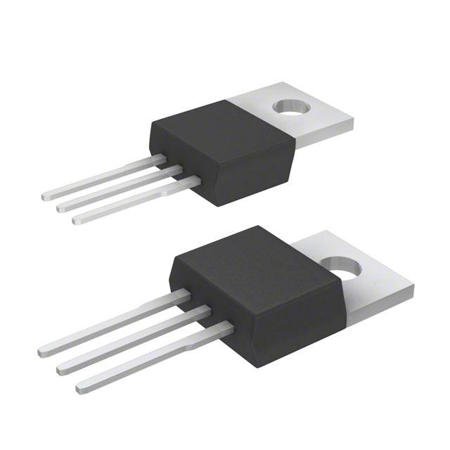
IPP200N25N3GXKSA1 is listed in the Single FETs, MOSFETs range at ChipApex. The manufacturer field lists Infineon Technologies. Its product description is MOSFET N-CH 250V 64A TO220-3. Review the specifications below when checking this part for your BOM.
The IPP200N25N3GXKSA1 is an N-channel Power MOSFET from the OptiMOS 3 family, housed in a PG-TO220-3 package. It features a drain-source voltage of 250 V and a continuous drain current of 64 A at 25 °C case temperature. The maximum on-resistance is 20 mΩ at VGS=10 V and ID=64 A. Total gate charge is typically 64 nC and maximally 86 nC. Thermal resistance junction-to-case is 0.5 K/W. Operating and storage temperatures range from -55 °C to +175 °C.
Verify the specific ordering suffix against official Infineon documentation to confirm exact packaging and marking details. Ensure that the procurement channel provides valid traceability data consistent with automotive or industrial grade requirements. Confirm compliance with JEDEC qualification standards relevant to the target application environment before finalizing orders.
Select this component when designing circuits requiring robust 250 V blocking capability combined with low conduction losses. Evaluate thermal management strategies based on the 0.5 K/W junction-to-case resistance. Consider the total gate charge characteristics for driver selection in high-speed switching topologies. Verify safe operating area limits under pulsed current conditions.
This device belongs to the OptiMOS 3 generation of silicon power transistors manufactured by Infineon Technologies. It shares core electrical specifications with the IPB200N25N3G (PG-TO263-3) and IPI200N25N3G (PG-TO262-3) variants, differing primarily in the physical lead frame and package outline used for PCB mounting.
Direct functional equivalents include IPB200N25N3G and IPI200N25N3G. These parts share identical electrical ratings but utilize different packages. Verify footprint compatibility and thermal interface requirements before substitution.
The device supports a single-pulse avalanche energy of 320 mJ when driven at 47 A with a gate resistance of 25 Ω.
The drain-source on-state resistance increases significantly as the junction temperature rises from 25 °C to 175 °C, following standard positive temperature coefficient behavior for silicon MOSFETs.
Input capacitance is typically 5340 pF, output capacitance is typically 297 pF, and reverse transfer capacitance is typically 4 pF, measured at VDS=100 V and f=1 MHz.
Explore related parts through FETs, MOSFETs, Transistors, Discrete Semiconductor Products, all product categories.
 IPP200N25N3GXKSA1

The activity of extra discounts on wholesale prices is in full swing…
Please fill in your contact information and we will send you the latest wholesale price list.