 ChipApex | Global Electronic Components Supplier

SEARCH
Search Product
Search Post
— IC芯片 | 连接器 | 传感器 | 被动器件 —
Search productSearch post
— IC芯片 | 连接器 | 传感器 | 被动器件 —
Consult the customer manager about the wholesale price.
consultation hotline:86-132-6715-2157
email:[email protected]
Contact the product manager for consultation. One-stop consultation is available.
Do you want a lower wholesale price? Please send us your inquiry and we will reply immediately.
IRF7101PBF is listed in the FET, MOSFET Arrays range at ChipApex. The manufacturer field lists Infineon Technologies. Its product description is MOSFET 2N-CH 20V 3.5A 8SO. Review the specifications below when checking this part for your BOM.
The IRF7101PBF is a dual N-channel HEXFET power MOSFET in an SO-8 package. It features a drain-source voltage of 20 V and a continuous drain current of 5.3 A at 25°C, or 4.9 A at 70°C. The maximum on-resistance is 0.10 Ω at VGS = 10 V and 0.18 Ω at VGS = 4.5 V. Total gate charge is typically 13 nC at VGS = 10 V. Power dissipation reaches 2.0 W at 25°C with a thermal resistance (junction-to-ambient) of 62.5 °C/W. Operating temperature ranges from -55°C to +150°C.
Verify the component origin carefully as Infineon acquired International Rectifier. Confirm the datasheet version matches the specific manufacturing lot. Ensure the SO-8 package dimensions align with your PCB footprint requirements. Check for lead-free compliance markings on the package surface.
Select this part for low-voltage, high-current synchronous rectification where compact size is critical. The dual channel allows cost reduction by sharing common nodes. Evaluate thermal performance under pulsed conditions using the provided ZthJA curves. Ensure gate drive voltage supports the specified RDS(on) thresholds.
This component belongs to the fourth-generation HEXFET family from International Rectifier, now part of Infineon Technologies. These devices utilize advanced trench technology to minimize on-resistance. The SO-8 package provides a compact solution for surface-mount assembly, suitable for consumer electronics and industrial applications requiring efficient power switching.
IRF7101TRPBF: Identical electrical specifications and pinout; differs only in tape-and-reel packaging format instead of tube.
The total gate charge (Qg) is typically 13 nC when measured at a gate-source voltage of 10 V.
The SO-8 package offers a junction-to-ambient thermal resistance of 62.5 °C/W, allowing heat dissipation through the exposed pad and leads.
Yes, the datasheet includes specific test circuits and parameters for dynamic dv/dt rating and body diode forward recovery characteristics.
Explore related parts through FETs, MOSFETs, Transistors, Discrete Semiconductor Products, all product categories.
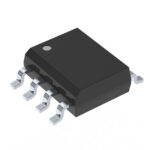 IRF7101PBF

The activity of extra discounts on wholesale prices is in full swing…
Please fill in your contact information and we will send you the latest wholesale price list.





