 ChipApex | Global Electronic Components Supplier

SEARCH
Search Product
Search Post
— IC芯片 | 连接器 | 传感器 | 被动器件 —
Search productSearch post
— IC芯片 | 连接器 | 传感器 | 被动器件 —
Consult the customer manager about the wholesale price.
consultation hotline:86-132-6715-2157
email:[email protected]
Contact the product manager for consultation. One-stop consultation is available.
Do you want a lower wholesale price? Please send us your inquiry and we will reply immediately.
IRF7329TRPBF is listed in the FET, MOSFET Arrays range at ChipApex. The manufacturer field lists Infineon Technologies. Its product description is MOSFET 2P-CH 12V 9.2A 8SO. Review the specifications below when checking this part for your BOM.
The IRF7329TRPBF is a dual P-channel HEXFET power MOSFET manufactured by Infineon Technologies. It features a -12V drain-source voltage rating and supports a continuous drain current of -9.2A at 25°C. The device utilizes trench technology to achieve an ultra-low on-resistance, with a maximum RDS(on) of 17mΩ at VGS = -4.5V. Packaged in a low-profile SO-8 format, it offers a power dissipation capacity of 2.0W at 25°C and operates within a junction temperature range of -55°C to +150°C.
Verify the component origin carefully as Infineon acquired International Rectifier. Ensure the datasheet corresponds to the specific manufacturer marking. Confirm that the application environment remains within the specified thermal limits and voltage ratings defined in the official specifications.
Select this component when a dual P-channel solution is required in a small footprint. Evaluate the thermal resistance characteristics against the expected ambient conditions. Compare the gate charge parameters against the driving capability of the control logic to ensure adequate switching performance.
This part belongs to the HEXFET family of power MOSFETs known for ruggedized device designs. The SO-8 package variant includes a customized leadframe to enhance thermal characteristics and support multiple-die capabilities, distinguishing it from standard single-transistor packages.
Direct pin-compatible replacements include the IRF7329PbF. Verify that any substitute maintains the -12V voltage rating and matches the SO-8 package dimensions for mechanical fit.
The absolute maximum gate-to-source voltage is rated at ±8.0V.
Yes, the internal MOSFET structure includes an integral reverse p-n junction diode between the source and drain.
The typical total gate charge (Qg) is 38nC under standard test conditions.
Explore related parts through FETs, MOSFETs, Transistors, Discrete Semiconductor Products, all product categories.
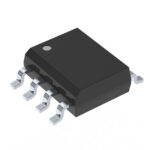 IRF7329TRPBF

The activity of extra discounts on wholesale prices is in full swing…
Please fill in your contact information and we will send you the latest wholesale price list.





