 ChipApex | Global Electronic Components Supplier

SEARCH
Search Product
Search Post
— IC芯片 | 连接器 | 传感器 | 被动器件 —
Search productSearch post
— IC芯片 | 连接器 | 传感器 | 被动器件 —
Consult the customer manager about the wholesale price.
consultation hotline:86-132-6715-2157
email:[email protected]
Contact the product manager for consultation. One-stop consultation is available.
Do you want a lower wholesale price? Please send us your inquiry and we will reply immediately.
IRF7342PBF is listed in the FET, MOSFET Arrays range at ChipApex. The manufacturer field lists Infineon Technologies. Its product description is MOSFET 2P-CH 55V 3.4A 8SO. Review the specifications below when checking this part for your BOM.
The IRF7342PBF is a dual P-channel power MOSFET from the Fifth Generation HEXFET series, manufactured by Infineon Technologies. It features a maximum drain-source voltage (VDS) of -55 V and a continuous drain current (ID) of -3.4 A at 25°C. The device offers an ultra-low on-resistance (RDS(on)) with a maximum value of 0.105 Ω at VGS = -10 V. Packaged in a surface-mount SO-8 format, it supports a junction temperature range of -55°C to +150°C and includes dynamic dv/dt rating capabilities for robust switching performance.
Verify component authenticity through official Infineon channels or authorized distributors. Confirm RoHS compliance status and check for specific manufacturing date codes relevant to your supply chain requirements. Ensure storage conditions adhere to moisture sensitivity level guidelines to prevent package damage prior to soldering.
Select this component when a dual P-channel solution is required to minimize printed circuit board space. Evaluate the thermal resistance parameters against your system's heat dissipation capabilities. Consider the gate threshold voltage specifications to ensure compatibility with your logic-level drive signals.
This part belongs to the HEXFET Power MOSFET family, known for advanced processing techniques that achieve low on-resistance. The SO-8 package modification allows for multiple-die capability, enabling designers to integrate two independent devices into one footprint while maintaining high reliability and efficiency standards.
Consult official cross-reference documentation for verified substitutes. Verify pinout compatibility and electrical parameter equivalence before implementation.
Explore related parts through FETs, MOSFETs, Transistors, Discrete Semiconductor Products, all product categories.
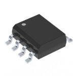 IRF7342PBF

The activity of extra discounts on wholesale prices is in full swing…
Please fill in your contact information and we will send you the latest wholesale price list.





