 ChipApex | Global Electronic Components Supplier

SEARCH
Search Product
Search Post
— IC芯片 | 连接器 | 传感器 | 被动器件 —
Search productSearch post
— IC芯片 | 连接器 | 传感器 | 被动器件 —
Consult the customer manager about the wholesale price.
consultation hotline:86-132-6715-2157
email:[email protected]
Contact the product manager for consultation. One-stop consultation is available.
Do you want a lower wholesale price? Please send us your inquiry and we will reply immediately.
IRF8513PBF is listed in the FET, MOSFET Arrays range at ChipApex. The manufacturer field lists Infineon Technologies. Its product description is MOSFET 2N-CH 30V 8A/11A 8SO. Review the specifications below when checking this part for your BOM.
The IRF8513PbF is a dual N-channel HEXFET Power MOSFET in an SO-8 package. It integrates two optimized transistors: Q1 (Control FET) with RDS(on) max 15.5 mΩ and ID 8.0 A, and Q2 (Synchronous FET) with RDS(on) max 12.7 mΩ and ID 11 A at VGS=10V. Both channels feature a BVDSS of 30 V, VGS(max) ±20 V, and TJ(max) 175°C. Q1 has PD 1.5 W and RθJA 100°C/W; Q2 has PD 2.4 W and RθJA 62.5°C/W.
Verify the component matches the exact Infineon/IR part number IRF8513PbF. Confirm the package type is SO-8 and the suffix PbF indicates lead-free compliance. Check the moisture sensitivity level and RoHS status against your manufacturing requirements. Ensure the supplier provides valid traceability documentation for this specific dual MOSFET variant.
Select this component when a compact dual-N-channel solution is required for low-voltage synchronous rectification. The device offers distinct control and synchronous FET characteristics within a single package. Evaluate thermal performance based on the specific junction-to-ambient resistance values for each channel under your PCB layout constraints.
This device belongs to the HEXFET family from Infineon Technologies (formerly International Rectifier). It utilizes advanced silicon technology to achieve low on-resistance per unit area. The dual configuration allows for space-saving designs in portable electronics where board real estate is limited compared to discrete single-channel alternatives.
No public confirmed substitute part numbers are available in the provided documentation.
Both Q1 and Q2 have a maximum drain-to-source breakdown voltage (BVDSS) of 30 V.
Q1 supports a continuous drain current of 8.0 A, while Q2 supports 11 A, both measured at VGS = 10V and TA = 25°C.
The maximum gate-to-source voltage (VGS) is rated at ±20 V for both channels.
Explore related parts through FETs, MOSFETs, Transistors, Discrete Semiconductor Products, all product categories.
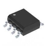 IRF8513PBF

The activity of extra discounts on wholesale prices is in full swing…
Please fill in your contact information and we will send you the latest wholesale price list.





