 ChipApex | Global Electronic Components Supplier
SEARCH
Search Product
Search Post
— IC芯片 | 连接器 | 传感器 | 被动器件 —
Search productSearch post
— IC芯片 | 连接器 | 传感器 | 被动器件 —
Consult the customer manager about the wholesale price.
consultation hotline:86-132-6715-2157
email:[email protected]
Contact the product manager for consultation. One-stop consultation is available.
Do you want a lower wholesale price? Please send us your inquiry and we will reply immediately.
The J110G is an N-channel silicon small-signal Junction Field-Effect Transistor (JFET) manufactured by onsemi. It utilizes a TO-92 three-lead plastic package designed for general-purpose amplification and switching applications. The device operates in depletion mode with a maximum drain-source voltage rating of 50 V and a continuous drain current capability of 100 mA. Key electrical characteristics include a minimum gate cutoff voltage (V_GS(off)) of -0.5 V and a maximum value of -6 V, ensuring predictable biasing across production lots. The component supports a maximum power dissipation of 310 mW at 25°C ambient temperature and functions within a junction temperature range of -55°C to +150°C.
Verify the specific ordering suffix against the manufacturer's official datasheet to confirm pinout orientation and electrical tolerances. Ensure that the procurement channel provides traceable documentation confirming RoHS compliance status. Cross-reference the part number with the latest onsemi product change notices to validate manufacturing origin and material composition before finalizing supply agreements.
Select this component when designing circuits requiring moderate voltage handling with low leakage current characteristics. Evaluate the gate cutoff voltage spread (-0.5 V to -6 V) to determine if external biasing networks are necessary for consistent performance. Compare the 100 mA drain current limit against peak load requirements to ensure adequate safety margins during transient conditions.
The J110G belongs to the standard discrete JFET family utilized in linear electronics design. It serves as a direct replacement for legacy N-channel JFETs in established amplifier topologies. The device maintains compatibility with common through-hole mounting techniques while offering reliable performance in consumer and industrial control systems requiring stable field-effect transistor behavior.
Publicly confirmed substitute part numbers include the 2N5457, J111, and J112. When substituting, verify that the alternative device matches the required gate cutoff voltage polarity and magnitude. Confirm that the replacement package maintains identical pin configuration to prevent PCB footprint modifications.
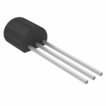 J110G
J110G
The activity of extra discounts on wholesale prices is in full swing…
Please fill in your contact information and we will send you the latest wholesale price list.





