 ChipApex | Global Electronic Components Supplier
SEARCH
Search Product
Search Post
— IC芯片 | 连接器 | 传感器 | 被动器件 —
Search productSearch post
— IC芯片 | 连接器 | 传感器 | 被动器件 —
Consult the customer manager about the wholesale price.
consultation hotline:86-132-6715-2157
email:[email protected]
Contact the product manager for consultation. One-stop consultation is available.
Do you want a lower wholesale price? Please send us your inquiry and we will reply immediately.
The onsemi J112_D11Z is an N-channel silicon Junction Field-Effect Transistor (JFET) designed for low-level analog switching applications. It operates in a depletion mode with a single configuration housed in a TO-92-3 package featuring kinked leads for through-hole mounting. Key electrical parameters include a drain-source current (Ids) of 5 mA, a maximum drain-source resistance (Rds) of 50 Ω, and a power dissipation (Pd) rating of 625 mW. The device supports a wide operating temperature range from -55°C to 150°C.
Verify the specific suffix _D11Z against the manufacturer's official datasheet to confirm lead style and packaging variations. Ensure the procurement channel provides traceability documentation required for industrial or medical-grade deployments. Cross-reference the RoHS compliance status with the latest environmental declarations before finalizing orders.
Select this component when designing circuits requiring low leakage and high linearity in analog signal paths. The TO-92 package is suitable for prototyping and low-volume production where through-hole reliability is prioritized over surface-mount density. Evaluate thermal management requirements given the 625 mW dissipation limit in enclosed environments.
This part belongs to the J112 series of N-channel JFETs originally developed for chopper transistor applications. The series includes variants such as J111 and J113, which share similar structural designs but may differ in specific electrical tolerances or pinout configurations. The D11Z suffix typically denotes specific mechanical or packaging attributes within the onsemi portfolio.
Direct substitutes include the MMBFJ112 for surface-mount implementations and other industry-standard N-channel JFETs like the 2N5457, provided pin compatibility and electrical ratings are verified against the specific application constraints.
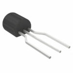 J112_D11Z
The activity of extra discounts on wholesale prices is in full swing…
Please fill in your contact information and we will send you the latest wholesale price list.






