ChipApex | Global Electronic Components Supplier
SEARCH
Search Product
Search Post
— IC芯片 | 连接器 | 传感器 | 被动器件 —
Search productSearch post
— IC芯片 | 连接器 | 传感器 | 被动器件 —
Consult the customer manager about the wholesale price.
consultation hotline:86-132-6715-2157
email:[email protected]
Contact the product manager for consultation. One-stop consultation is available.
Do you want a lower wholesale price? Please send us your inquiry and we will reply immediately.
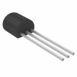
The J174 is a P-Channel Silicon Junction Field Effect Transistor (JFET) designed for low-level analog switching applications. It is available in TO-92 and SOT-23 packages. Key electrical characteristics include a Drain-Gate Voltage of -30 V, Gate-Source Voltage of 30 V, and a Zero-Gate Voltage Drain Current (IDSS) range of -20 mA to -100 mA at VDS = -15 V. The device features a Drain-Source On Resistance (rDS(on)) maximum of 85 Ω and a Gate-Source Cutoff Voltage (VGS(off)) range of 5.0 V to 10 V. Total device dissipation is 350 mW in the TO-92 package.
Verify the specific package variant required, as the J174 is manufactured in both TO-92 and SOT-23 configurations with distinct pinouts and thermal characteristics. Confirm that the ordering suffix corresponds to the desired packaging style, such as tape and reel or bulk, as these do not alter the electrical function but affect handling and assembly processes. Ensure compatibility with the intended PCB footprint before procurement.
Select the J174 when a P-Channel JFET with high IDSS and low rDS(on) is required for precision analog switching. Compare against J175, J176, and J177 if different IDSS or VGS(off) ranges are needed to match specific circuit thresholds. Consider the SOT-23 version for surface-mount designs requiring smaller footprints, while retaining TO-92 for through-hole applications needing higher power dissipation capabilities.
The J174 belongs to the J174/J175/J176/J177 family of P-Channel Switches originally developed by Fairchild Semiconductor. This family shares identical physical dimensions and pinouts but varies in electrical parameters like IDSS and VGS(off) to provide options for different switching speeds and leakage requirements. The MMBFJ17x series represents the surface-mount equivalent of this family.
Direct functional substitutes within the same family include J175, J176, and J177, which share the same package and pinout but offer different IDSS and VGS(off) specifications. Surface-mount replacements include the MMBFJ174, MMBFJ175, MMBFJ176, and MMBFJ177 in SOT-23 packages. Verify parameter compatibility before substitution.
Yes, the datasheet explicitly notes that the source and drain terminals are interchangeable, allowing for flexible circuit orientation.
The absolute maximum Drain-Gate Voltage (VDG) rating for the J174 is -30 V.
The primary difference lies in their electrical characteristics. The J174 has a higher IDSS range (-20 mA to -100 mA) and a higher VGS(off) range (5.0 V to 10 V) compared to the J175, which has lower values for these parameters.

The activity of extra discounts on wholesale prices is in full swing…
Please fill in your contact information and we will send you the latest wholesale price list.