ChipApex | Global Electronic Components Supplier
SEARCH
Search Product
Search Post
— IC芯片 | 连接器 | 传感器 | 被动器件 —
Search productSearch post
— IC芯片 | 连接器 | 传感器 | 被动器件 —
Consult the customer manager about the wholesale price.
consultation hotline:86-132-6715-2157
email:[email protected]
Contact the product manager for consultation. One-stop consultation is available.
Do you want a lower wholesale price? Please send us your inquiry and we will reply immediately.
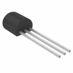
The onsemi J175 is a P-Channel Junction Field Effect Transistor (JFET) switch designed for low-level analog applications. It operates within a Drain-Gate voltage of -30 V and a Gate-Source voltage of 30 V. The device features a maximum zero-gate voltage drain current (IDSS) of -7.0 mA and a typical drain-source on resistance (rDS(on)) of 125 Ω at VGS = 0. It supports an operating junction temperature range from -55°C to +150°C with a total device dissipation of 350 mW.
Verify the specific package variant required, as the J175 is available in SOT-23 and TO-92 configurations. Confirm that the sourcing channel provides original manufacturer documentation to ensure the component meets the specified electrical characteristics, particularly the IDSS and rDS(on) tolerances defined in the datasheet.
Select the J175 when designing circuits requiring precise analog signal routing with minimal leakage. Consider the 125 Ω on-resistance for impedance matching requirements. Ensure the application stays within the 350 mW power dissipation limit and utilizes the appropriate thermal derating curves for ambient temperatures exceeding 25°C.
The J175 belongs to a family of P-Channel JFET switches that includes the J174, J176, and J177 models. These devices are sourced from Process 88 and share similar structural characteristics but differ in their specific IDSS and rDS(on) ranges to accommodate various analog switching needs.
Direct substitutes include the MMBFJ175 for surface mount implementations or other J-series P-Channel JFETs with comparable IDSS and breakdown voltage ratings. Verify pinout compatibility and thermal performance before substitution.
No, the source and drain terminals are interchangeable, allowing for flexible orientation during circuit assembly.
The maximum operating and storage junction temperature range is -55°C to +150°C.
The gate reverse current (IGSS) is limited to a maximum of 1.0 nA when VGS is 20 V and VDS is 0 V.

The activity of extra discounts on wholesale prices is in full swing…
Please fill in your contact information and we will send you the latest wholesale price list.