ChipApex | Global Electronic Components Supplier
SEARCH
Search Product
Search Post
— IC芯片 | 连接器 | 传感器 | 被动器件 —
Search productSearch post
— IC芯片 | 连接器 | 传感器 | 被动器件 —
Consult the customer manager about the wholesale price.
consultation hotline:86-132-6715-2157
email:[email protected]
Contact the product manager for consultation. One-stop consultation is available.
Do you want a lower wholesale price? Please send us your inquiry and we will reply immediately.
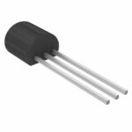
The onsemi J177 is a P-Channel Silicon Junction Field Effect Transistor (JFET) designed for low-level analog switching applications. It operates within a drain-source voltage range of -30 V and supports a junction temperature up to +150 °C. The device features a zero-gate voltage drain current (IDSS) ranging from -20 mA to -100 mA at VDS = -15 V, with a maximum drain-source on-resistance (rDS(on)) of 300 Ω. It is available in TO-92 and SOT-23 packages.
Verify the specific package variant required, as the J177 is available in both TO-92 and SOT-23 configurations. Confirm that the IDSS bin matches the design requirements, as the datasheet specifies a wide range from -20 mA to -100 mA. Ensure the sourcing entity is authorized, noting the historical transition from Fairchild Semiconductor to onsemi for this product line.
Select the J177 when designing precision analog signal paths requiring low leakage and high input impedance. Consider the wide IDSS variation (-20 mA to -100 mA) during circuit simulation to ensure consistent cutoff behavior across different units. Evaluate thermal dissipation limits if operating near the maximum junction temperature of 150 °C.
The J177 belongs to a family of P-Channel JFETs that includes the J174, J175, and J176, differentiated primarily by their IDSS bins. This series was originally manufactured by Fairchild Semiconductor and is now part of the onsemi portfolio. The devices are built on Process 88 silicon technology.
Direct substitutes include other parts from the same family such as the J174, J175, and J176, provided the specific IDSS bin requirements are met. Cross-reference MMBFJ177 for surface-mount equivalents in the SOT-23 package.
Yes, the datasheet explicitly notes that the source and drain terminals are interchangeable for the J177 device.
The maximum Gate-Source Breakdown Voltage (B(BR)GSS) is specified as 30 V.
The Drain-Source On Resistance (rDS(on)) varies based on the specific bin; for the J177, it has a maximum value of 300 Ω.

The activity of extra discounts on wholesale prices is in full swing…
Please fill in your contact information and we will send you the latest wholesale price list.