ChipApex | Global Electronic Components Supplier
SEARCH
Search Product
Search Post
— IC芯片 | 连接器 | 传感器 | 被动器件 —
Search productSearch post
— IC芯片 | 连接器 | 传感器 | 被动器件 —
Consult the customer manager about the wholesale price.
consultation hotline:86-132-6715-2157
email:[email protected]
Contact the product manager for consultation. One-stop consultation is available.
Do you want a lower wholesale price? Please send us your inquiry and we will reply immediately.
The LS26VNS is an N-Channel JFET voltage controlled resistor with a drain-source resistance managed by a DC bias voltage applied to the gate. It operates within a junction temperature range of -55°C to +135°C and supports continuous power dissipation of 350mW at 25°C. The device provides a predictable RDS change from 14Ω to 38Ω as VGS approaches pinch-off, maintaining performance without VGS variation. Key electrical parameters include a gate-to-source breakdown voltage of -40V, input capacitance of 13pF, and reverse transfer capacitance of 3.6pF.
Verify the specific package variant (TO-92, SOT-23, or DFN) matches the design footprint. Confirm RoHS compliance status for environmental regulations. Ensure the selected part number suffix aligns with the required lead count and physical dimensions. Cross-reference absolute maximum ratings against system operating conditions to prevent serviceability impairment.
Select this component for low-level AC signal applications requiring no DC component on the drain-source path. Evaluate the static RDS(on) ratio of 0.90 to 1.0 for consistency needs. Consider the -40V gate-to-source breakdown voltage for high-voltage tolerance requirements. Verify that the 14Ω to 38Ω resistance range meets the specific attenuation or gain control specifications.
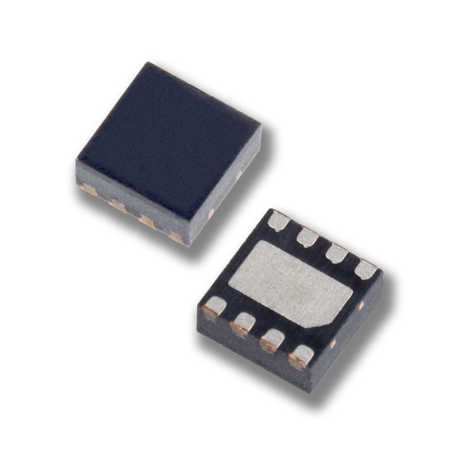
This component belongs to the LS26VNS series of N-Channel JFETs designed specifically as voltage controlled resistors. It is available in multiple packages including TO-92, SOT-23, and DFN. The series is engineered for applications demanding predictable resistance changes controlled by DC bias voltages on a high-impedance gate terminal.
Public confirmed substitute part numbers are not provided in the source documentation.
The minimum RDS is 14 Ω, which occurs when VGS is -1.0V.
It features simplified drive voltage capabilities and high input impedance, allowing control via a DC bias voltage applied to the gate terminal.
In the DFN 8L package, leads 1, 2, 4, 5, and 7 have no connection.
 LS26VNS DFN 8L ROHS
The activity of extra discounts on wholesale prices is in full swing…
Please fill in your contact information and we will send you the latest wholesale price list.