ChipApex | Global Electronic Components Supplier
SEARCH
Search Product
Search Post
— IC芯片 | 连接器 | 传感器 | 被动器件 —
Search productSearch post
— IC芯片 | 连接器 | 传感器 | 被动器件 —
Consult the customer manager about the wholesale price.
consultation hotline:86-132-6715-2157
email:[email protected]
Contact the product manager for consultation. One-stop consultation is available.
Do you want a lower wholesale price? Please send us your inquiry and we will reply immediately.
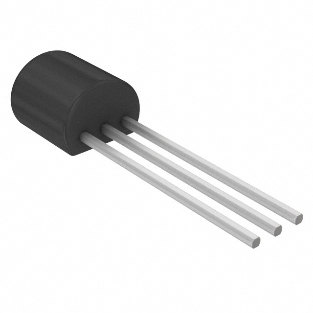
The LSK189 is a single N-channel JFET in a TO-92 package. It features an ultra-low noise voltage of 1.8 nV/√Hz at 1 kHz and low input capacitance of 4 pF. Key electrical parameters include a gate-to-source breakdown voltage of -60 V, a drain-to-source saturation current (IDSS) range of 2.5 to 15 mA, and a transconductance (Gfs) of 1500 µS. The device supports a continuous power dissipation of 300 mW at 25°C and operates within a junction temperature range of -55°C to +150°C.
Verify the component matches the specific Linear Integrated Systems datasheet revision A20. Confirm the package type is TO-92 and the RoHS compliance status aligns with project requirements. Ensure the ordering suffix corresponds to the correct packaging format. Cross-reference the part number against official manufacturer documentation to avoid counterfeit or obsolete stock.
Select this component when minimizing input-referred noise is critical. The low input capacitance makes it suitable for high-impedance sources. Verify that the IDSS range fits the biasing requirements of the target circuit. Consider the thermal derating characteristics if operating above 25°C ambient temperature.
Linear Integrated Systems specializes in high-performance discrete semiconductors using proprietary processes. The LSK189 belongs to a family of low-noise JFETs designed for precision analog applications. This specific model offers a balance of low noise and low capacitance in a standard through-hole package.
The LSK489 is documented as an equivalent monolithic dual version. Verify pinout compatibility and electrical parameter overlaps before substitution. No other direct substitutes are confirmed in the provided documentation.
The typical noise voltage is 1.8 nV/√Hz at 1 kHz.
The maximum gate-to-source voltage is -60 V.
The LSK189 is a single JFET. An equivalent monolithic dual is available as the LSK489.
 LSK189 TO-92 3L ROHS
The activity of extra discounts on wholesale prices is in full swing…
Please fill in your contact information and we will send you the latest wholesale price list.