ChipApex | Global Electronic Components Supplier
SEARCH
Search Product
Search Post
— IC芯片 | 连接器 | 传感器 | 被动器件 —
Search productSearch post
— IC芯片 | 连接器 | 传感器 | 被动器件 —
Consult the customer manager about the wholesale price.
consultation hotline:86-132-6715-2157
email:[email protected]
Contact the product manager for consultation. One-stop consultation is available.
Do you want a lower wholesale price? Please send us your inquiry and we will reply immediately.
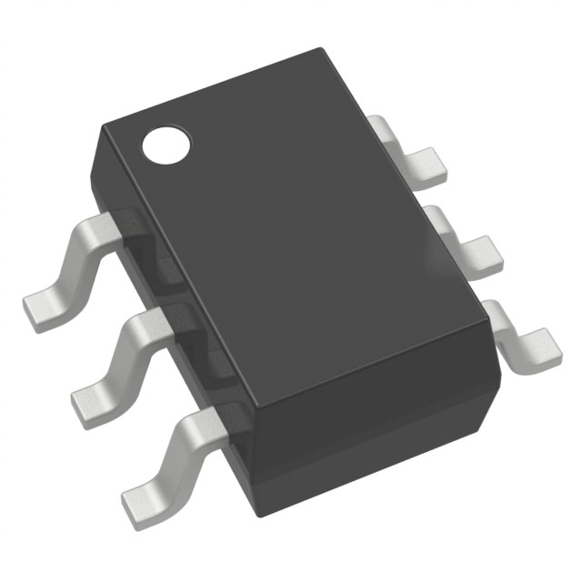
The LSK489B is a low-noise, monolithic dual N-channel JFET amplifier in a SOT-23 6L package. It features an input capacitance of 4pF and a noise voltage of 1.8nV/√Hz at 1kHz. The device offers a common mode rejection ratio of 102dB and operates with a gate-to-source breakdown voltage of 60V. Drain saturation current ranges from 8.0mA to 15.0mA, with a transconductance of 1500µS. It provides tight differential matching and low offset drift for precision applications.
Verify the specific ordering suffix matches the required performance grade. Confirm the package type aligns with the PCB footprint requirements. Ensure the component meets RoHS standards if mandated by the design specifications. Cross-reference the datasheet revision to confirm electrical parameters match the intended application constraints.
Select this component when minimizing input capacitance is critical for maintaining bandwidth and reducing distortion. The B-grade variant offers specific drain saturation current limits suitable for precise biasing requirements. Consider the SOT-23 package for space-constrained designs requiring surface mount technology.
This part belongs to the LSK489 series of low-noise dual JFETs. It serves as a high-performance alternative to standard discrete JFETs by offering matched pairs on a single die. The device complements the single-channel LSK189 and shares pin compatibility with the LSK389 in certain packages.
The LSK389 is a compatible replacement in TO-71 and SOIC packages due to identical fit, form, and pinout. Designers should verify that the slightly higher noise level of the LSK389 does not impact circuit sensitivity.
The typical common source input capacitance (CISS) is 4pF.
The LSK489 has a much lower gate-to-drain capacitance of 4pF compared to the 25pF found in the LSK389.
The maximum gate-to-source voltage (VGSS) is rated at 60V.
 LSK489B SOT-23 6L ROHS
The activity of extra discounts on wholesale prices is in full swing…
Please fill in your contact information and we will send you the latest wholesale price list.