 ChipApex | Global Electronic Components Supplier
SEARCH
Search Product
Search Post
— IC芯片 | 连接器 | 传感器 | 被动器件 —
Search productSearch post
— IC芯片 | 连接器 | 传感器 | 被动器件 —
Consult the customer manager about the wholesale price.
consultation hotline:86-132-6715-2157
email:[email protected]
Contact the product manager for consultation. One-stop consultation is available.
Do you want a lower wholesale price? Please send us your inquiry and we will reply immediately.
The MAX2602ESA+T is a silicon bipolar RF power transistor integrated with a thermally matched biasing diode, designed for portable cellular and wireless equipment. It delivers 1W of RF output power at 900MHz from a 3.6V supply with 58% collector efficiency in constant-envelope applications. For NADC (IS-54) operation, it provides 29dBm output with -28dBc ACPR from a 4.8V supply. The device operates within a DC-to-microwave frequency range, featuring a 17V collector-emitter breakdown voltage, 1.2A average collector current, and 6.4W continuous power dissipation. It is housed in an 8-pin SO package with an extended temperature range of -40°C to +85°C.
Verify component authenticity through authorized Analog Devices distributors. Confirm the presence of the '+' suffix indicates lead-free compliance. Ensure the SOIC-8 package includes the exposed thermal slug for proper soldering to the ground plane to meet the specified 6.4W power dissipation rating. Check for RoHS certification documentation prior to final procurement.
Select the MAX2602 over the MAX2601 when precise thermal tracking of the quiescent collector current is required. The internal biasing diode simplifies the design of temperature-compensated bias networks. Ensure the application matching network accounts for the specific optimum source and load impedances defined in the datasheet to achieve maximum efficiency and linearity.
This component belongs to the MAX2601/MAX2602 family of 3.6V, 1W RF power transistors optimized for 900MHz applications. While the MAX2601 contains only the RF power transistor, the MAX2602 variant integrates the additional biasing diode. Both share identical electrical performance regarding RF power gain, output power, and noise figure specifications.
The MAX2601ESA+T serves as a direct functional substitute if the integrated biasing diode is not utilized in the existing circuit design. Verify that the replacement part maintains the same 8-pin SO package configuration and thermal slug requirements for adequate heat dissipation.
The diode is a scaled version of the power transistor's base-emitter junction. Current through the diode is proportional to 1/15th of the quiescent collector current, allowing the bias network to maintain constant collector current despite temperature changes.
For maximum efficiency at VBB = 0.75V and VCC = 3.6V, the optimum source impedance is 5.5 + j2.0 ohms and the load impedance is 6.5 + j1.5 ohms.
No, a drain switch is not required. This eliminates wasted power from switching devices and allows for lower system end-of-life battery voltage operation.
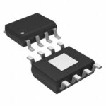 MAX2602ESA+T
The activity of extra discounts on wholesale prices is in full swing…
Please fill in your contact information and we will send you the latest wholesale price list.





