 ChipApex | Global Electronic Components Supplier
SEARCH
Search Product
Search Post
— IC芯片 | 连接器 | 传感器 | 被动器件 —
Search productSearch post
— IC芯片 | 连接器 | 传感器 | 被动器件 —
Consult the customer manager about the wholesale price.
consultation hotline:86-132-6715-2157
email:[email protected]
Contact the product manager for consultation. One-stop consultation is available.
Do you want a lower wholesale price? Please send us your inquiry and we will reply immediately.
The MMBF4391 is an N-channel JFET switch manufactured by onsemi, housed in a SOT-23 surface-mount package. It features a Drain-Gate Voltage of 30 V and a Gate-Source Voltage rating of -30 V. The device operates within a junction temperature range of -55°C to 150°C with a total power dissipation of 350 mW. Key electrical characteristics include a Zero-Gate Voltage Drain Current (IDSS) ranging from 50 mA to 150 mA at VDS = 20 V, and a Drain-Source On Resistance (rDS(on)) of 30 Ω at ID = 1.0 mA. The input capacitance (Ciss) is 14 pF.
Verify the specific part number suffix against official onsemi documentation to ensure correct packing method and top marking. Confirm that the component meets RoHS compliance requirements for your assembly process. Ensure sourcing channels are authorized distributors to guarantee genuine parts and full traceability. Validate all operating parameters for your specific application conditions before implementation.
Select this component when high drain current capability is required compared to standard JFETs. The MMBF4391 offers a higher IDSS range than the MMBF4392 or MMBF4393 variants. Consider the 30 Ω on-resistance and 14 pF input capacitance for signal integrity requirements. Verify thermal management capabilities given the 357 °C/W junction-to-ambient resistance.
This device belongs to the MMBF439x series of N-channel switches. It is sourced from Process 51 and shares characteristics with the J111 device. The series includes MMBF4392 and MMBF4393, which offer lower IDSS ranges. The product line is now managed by onsemi following the integration of Fairchild Semiconductor.
MMBF4392LT1G
The IDSS ranges from 50 mA to 150 mA when measured at VDS = 20 V and VGS = 0.
Yes, the datasheet notes that the source and drain leads are interchangeable.
The V(BR)GSS is specified as -30 V with a gate current of 1.0 μA and VDS = 0.
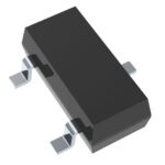 MMBF4391
The activity of extra discounts on wholesale prices is in full swing…
Please fill in your contact information and we will send you the latest wholesale price list.





