 ChipApex | Global Electronic Components Supplier
SEARCH
Search Product
Search Post
— IC芯片 | 连接器 | 传感器 | 被动器件 —
Search productSearch post
— IC芯片 | 连接器 | 传感器 | 被动器件 —
Consult the customer manager about the wholesale price.
consultation hotline:86-132-6715-2157
email:[email protected]
Contact the product manager for consultation. One-stop consultation is available.
Do you want a lower wholesale price? Please send us your inquiry and we will reply immediately.
The MMBFJ175 is a P-Channel Junction Field Effect Transistor (JFET) manufactured by onsemi. It features a Gate-Source Breakdown Voltage of 30 V and a Zero-Gate Voltage Drain Current range of -2.0 mA to -25.0 mA at VDS = -15 V. The device operates within a junction temperature range of -55 °C to +150 °C. Available in SOT-23 (TO-236) and TO-92 packages, it supports a maximum total device dissipation of 225 mW in the surface-mount configuration.
Verify the specific package variant required, as the datasheet lists both TO-92 and SOT-23 configurations under the J176/MMBFJ176 designation. Confirm that the ordering suffix matches the desired packing method, such as tape and reel or fan-fold. Ensure the component meets RoHS compliance standards if applicable to the assembly process. Cross-reference the marking diagram to validate the physical unit received against the ordered part number.
Select this component when a P-Channel JFET is required for precision analog signal routing. The interchangeable source and drain terminals provide layout flexibility. Consider the thermal resistance values when designing for high ambient temperatures. Verify that the gate-source cutoff voltage specifications align with the control logic levels used in the target circuit design.
This device belongs to the J176 family of P-Channel JFETs produced by onsemi. It is sourced from process 88, indicating a specific manufacturing lineage. The product line includes variants available in through-hole and surface-mount packages, catering to diverse PCB integration requirements for discrete semiconductor components.
MMBFJ176LT1G
Yes, the datasheet explicitly states that the source and drain are interchangeable.
The maximum operating and storage junction temperature range is up to +150 °C.
The gate reverse current is specified as a maximum of 1.0 nA at VGS = 20 V and VDS = 0.
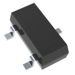 MMBFJ175
The activity of extra discounts on wholesale prices is in full swing…
Please fill in your contact information and we will send you the latest wholesale price list.





