 ChipApex | Global Electronic Components Supplier

SEARCH
Search Product
Search Post
— IC芯片 | 连接器 | 传感器 | 被动器件 —
Search productSearch post
— IC芯片 | 连接器 | 传感器 | 被动器件 —
Consult the customer manager about the wholesale price.
consultation hotline:86-132-6715-2157
email:[email protected]
Contact the product manager for consultation. One-stop consultation is available.
Do you want a lower wholesale price? Please send us your inquiry and we will reply immediately.
The MPC9352FA is a 3.3 V or 2.5 V compatible, 1:11 LVCMOS zero-delay clock generator designed for high-performance telecom, networking, and computing applications. It features a fully integrated PLL capable of generating output frequencies from 16.67 MHz to 200 MHz with maximum output skew below 200 ps. The device supports multiplication factors of 3, 2, 1, 3/2, 2/3, 1/3, and 1/2 via configurable FSEL pins across three output banks. It operates within an ambient temperature range of -40°C to +85°C and is housed in a 32-lead LQFP package.
Verify the specific suffix 'FA' against manufacturer documentation to confirm lead-free status and exact package variant, as suffixes may denote material or environmental compliance differences. Confirm current availability status as this component series may be subject to discontinuation notices.
Select based on required output frequency range (16.67–200 MHz) and voltage compatibility (2.5 V or 3.3 V). Ensure the application requires up to 11 outputs with low skew (<200 ps). Verify that the input reference frequency allows the VCO to remain within its 200–400 MHz lock range using the available feedback dividers.
The MPC9352 belongs to the Freescale Semiconductor (now NXP) Advanced Clock Drivers family. It is specifically engineered as a low-voltage clock generator and driver for complex clock trees where phase alignment and minimal jitter are critical for system synchronization.
Publicly confirmed substitute part numbers are not available in the provided source material. Consult official distributor databases for cross-reference data.
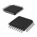 MPC9352FA

The activity of extra discounts on wholesale prices is in full swing…
Please fill in your contact information and we will send you the latest wholesale price list.






