ChipApex | Global Electronic Components Supplier
SEARCH
Search Product
Search Post
— IC芯片 | 连接器 | 传感器 | 被动器件 —
Search productSearch post
— IC芯片 | 连接器 | 传感器 | 被动器件 —
Consult the customer manager about the wholesale price.
consultation hotline:86-132-6715-2157
email:[email protected]
Contact the product manager for consultation. One-stop consultation is available.
Do you want a lower wholesale price? Please send us your inquiry and we will reply immediately.
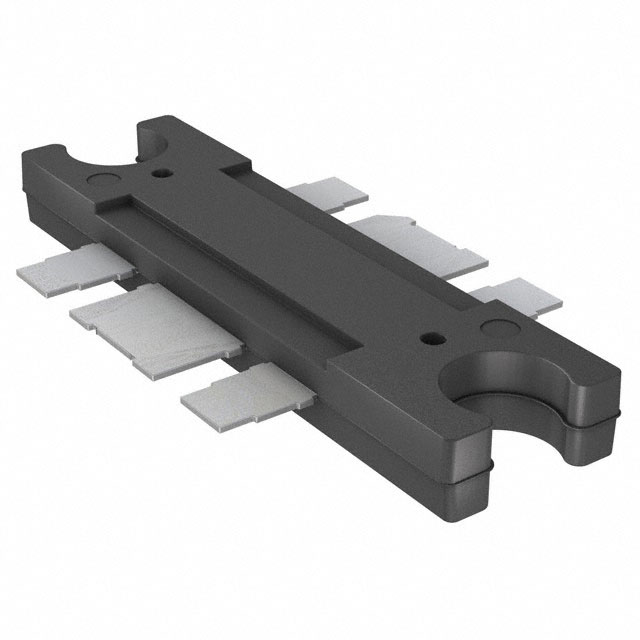
The MRF1550FNT1 is an N-Channel Enhancement-Mode Lateral MOSFET designed for broadband commercial and industrial applications with frequencies up to 175 MHz. It delivers 50 Watts of output power at 12.5 Volts with a power gain of 14.5 dB and drain efficiency of 55%. The device withstands 20:1 VSWR under overdrive conditions, features a TO-272-6 wrap plastic package, and operates within a junction temperature range up to 200 °C.
Verify the specific ordering suffix 'T1' corresponds to the tape and reel packaging configuration containing 500 units per 44 mm reel. Confirm that the component meets RoHS compliance standards and utilizes lead-free terminations as indicated by the 'N' suffix in the part number. Ensure the source documentation matches the Freescale Semiconductor datasheet revision history for accurate electrical specifications.
Select this component for applications requiring high gain and stable operation in common-source amplifier configurations. The device is optimized for 12.5 Volt supply rails and requires careful heat sinking due to its surface mount package. Designers should account for the lack of internal gate protection and implement external Zener diodes or resistive loading to ensure circuit stability against voltage transients.
Originally manufactured by Freescale Semiconductor, this device belongs to the MRF1550 series of RF power lateral MOSFETs. The product line was subsequently integrated into NXP Semiconductors following corporate acquisitions. The MRF1550FNT1 variant specifically denotes the tape and reel packaging format intended for automated surface mount assembly processes.
Direct replacements include the MRF1550NT1, which shares identical electrical characteristics but may differ in packaging format. Verify compatibility regarding the TO-272-6 case outline dimensions and pin assignments before substituting components in existing board layouts.
No, the device does not contain an internal monolithic Zener diode. External gate protection using a Zener diode or resistor is recommended to prevent oxide layer damage from voltage transients.
The maximum operating junction temperature (TJ) is specified as 200 °C.
Since the gate draws negligible DC current, the bias circuit generally consists of a simple resistive divider network. Special linear applications may require more elaborate biasing to optimize critical parameters.
 MRF1550FNT1
The activity of extra discounts on wholesale prices is in full swing…
Please fill in your contact information and we will send you the latest wholesale price list.