ChipApex | Global Electronic Components Supplier
SEARCH
Search Product
Search Post
— IC芯片 | 连接器 | 传感器 | 被动器件 —
Search productSearch post
— IC芯片 | 连接器 | 传感器 | 被动器件 —
Consult the customer manager about the wholesale price.
consultation hotline:86-132-6715-2157
email:[email protected]
Contact the product manager for consultation. One-stop consultation is available.
Do you want a lower wholesale price? Please send us your inquiry and we will reply immediately.
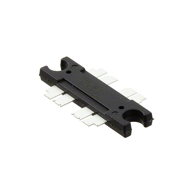
The MRF1570FNT1 is an N-Channel Enhancement-Mode Lateral MOSFET designed for broadband commercial and industrial applications up to 470 MHz. It operates at a drain-source voltage of 12.5 Vdc, delivering 70 W output power with 11.5 dB gain and 60% efficiency at 470 MHz. The device withstands 20:1 VSWR under overdrive conditions. Maximum ratings include a drain-source voltage of +40 Vdc, total device dissipation of 165 W at 25°C case temperature, and an operating junction temperature up to 200°C.
Verify the component matches the specific Freescale Semiconductor datasheet revision 10 (June 2009). Confirm the package style corresponds to Case 1366A-03 (TO-272-8 Wrap Plastic) and that the suffix FNT1 indicates lead-free terminations and tape-and-reel packaging. Ensure compatibility with the specified 12.5 Vdc supply requirements.
Select this device for designs requiring high gain and wide bandwidth without complex tuning networks. The lateral MOSFET structure offers immunity from thermal runaway and simplified biasing compared to bipolar alternatives. Verify that the application can accommodate the required quiescent current of 800 mA and that the PCB layout supports the necessary heat sinking for the plastic package.
This component belongs to the MRF1570 series of RF power transistors manufactured by Freescale Semiconductor. It serves as a surface-mount solution for VHF and UHF mobile power amplifier applications, replacing older through-hole variants while maintaining form, fit, and function compatibility.
The MRF1570T1 and MRF1570FT1 are confirmed replacements with no form, fit, or function changes.
No, the device does not contain an internal monolithic Zener diode. External protection is recommended if gate voltage transients are expected.
The maximum operating junction temperature is 200°C.
The gate must never be left open-circuited or floating. It should be terminated with a low impedance path to prevent turn-on due to leakage currents or voltage buildup.
 MRF1570FNT1
The activity of extra discounts on wholesale prices is in full swing…
Please fill in your contact information and we will send you the latest wholesale price list.