 ChipApex | Global Electronic Components Supplier
SEARCH
Search Product
Search Post
— IC芯片 | 连接器 | 传感器 | 被动器件 —
Search productSearch post
— IC芯片 | 连接器 | 传感器 | 被动器件 —
Consult the customer manager about the wholesale price.
consultation hotline:86-132-6715-2157
email:[email protected]
Contact the product manager for consultation. One-stop consultation is available.
Do you want a lower wholesale price? Please send us your inquiry and we will reply immediately.
The MRF5S9070NR1 is an N-channel enhancement-mode lateral MOSFET designed for broadband commercial and industrial applications up to 1000 MHz. It operates at a drain-source voltage of 68 Vdc with a typical power gain of 17.8 dB at 880 MHz. The device delivers 14 Watts average output power in Single-Carrier N-CDMA configurations and supports 60 Watts CW output in GSM bands. It features integrated ESD protection, lead-free terminations, and a TO-270-2 plastic package.
Verify the specific datasheet revision against the manufacturer's official records before implementation. Confirm that the R1 suffix corresponds to the required tape and reel quantity of 500 units per 24 mm reel. Ensure thermal management designs account for the specified junction-to-case resistance values under varying case temperatures.
Select this component for high-gain, broadband RF power amplification requiring robust ruggedness. Evaluate thermal constraints carefully, as the device supports high junction temperatures up to 200°C. Verify impedance matching networks using the provided series equivalent large-signal impedance parameters for optimal performance across the target frequency band.
This part belongs to the Freescale Semiconductor RF Power Field Effect Transistor family. It utilizes Lateral N-Channel technology optimized for 26-volt base station environments. The device is housed in a TO-270-2 plastic package, designated as Case 1265-09, Style 1, providing a compact form factor for high-power density applications.
Consult official documentation for direct substitutes within the same product family. Cross-referencing requires matching electrical characteristics, package dimensions, and thermal properties to ensure functional compatibility without redesigning the host circuitry.
The maximum operating junction temperature is 200°C.
It is packaged in a TO-270-2 plastic package (Case 1265-09).
Yes, the MRF5S9070NR1 includes integrated ESD protection characterized by Human Body Model Class 2 and Machine Model Class A.
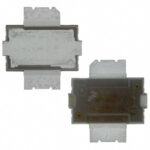 MRF5S9070NR1
The activity of extra discounts on wholesale prices is in full swing…
Please fill in your contact information and we will send you the latest wholesale price list.





