 ChipApex | Global Electronic Components Supplier
SEARCH
Search Product
Search Post
— IC芯片 | 连接器 | 传感器 | 被动器件 —
Search productSearch post
— IC芯片 | 连接器 | 传感器 | 被动器件 —
Consult the customer manager about the wholesale price.
consultation hotline:86-132-6715-2157
email:[email protected]
Contact the product manager for consultation. One-stop consultation is available.
Do you want a lower wholesale price? Please send us your inquiry and we will reply immediately.
The MRF6V12500HSR3 is a lateral N-channel RF power LDMOS transistor designed for pulsed applications operating between 960 and 1215 MHz. It delivers a peak output power of 500 W at 50 V drain-source voltage. The device features an internally matched input and output, eliminating the need for external matching networks. It is characterized with series equivalent large-signal impedance parameters and includes integrated ESD protection. The component utilizes the NI-780S-2L package.
Verify the specific ordering suffix against the manufacturer's current documentation to confirm the correct tape and reel configuration. Confirm that the intended application environment remains within the specified thermal limits, as continuous use at maximum temperatures affects mean time to failure. Ensure compatibility with the NI-780S-2L package outline during mechanical integration.
Select this component when designing systems requiring high peak power in the 960 to 1215 MHz band. The internal matching reduces component count and layout complexity compared to unmatched devices. Consider the thermal impedance characteristics and junction temperature limits when determining heat sink requirements for sustained pulsed duty cycles.
This part belongs to the MRF6V12500H family of RF power LDMOS transistors manufactured by NXP Semiconductors. The HS suffix indicates the specific NI-780S-2L surface mount package variant. This family is engineered specifically for aviation and radar frequencies where high reliability and pulse handling capabilities are critical.
MRF6V12500HR5
The Drain-Source Breakdown Voltage (V(BR)DSS) is 110 Vdc.
No, the device is internally matched on both the input and output sides.
The typical power gain (Gps) is 19.7 dB under narrowband short pulse conditions.
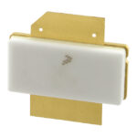 MRF6V12500HSR3
The activity of extra discounts on wholesale prices is in full swing…
Please fill in your contact information and we will send you the latest wholesale price list.





