ChipApex | Global Electronic Components Supplier
SEARCH
Search Product
Search Post
— IC芯片 | 连接器 | 传感器 | 被动器件 —
Search productSearch post
— IC芯片 | 连接器 | 传感器 | 被动器件 —
Consult the customer manager about the wholesale price.
consultation hotline:86-132-6715-2157
email:[email protected]
Contact the product manager for consultation. One-stop consultation is available.
Do you want a lower wholesale price? Please send us your inquiry and we will reply immediately.
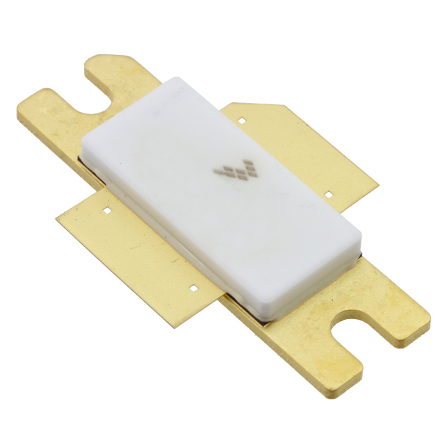
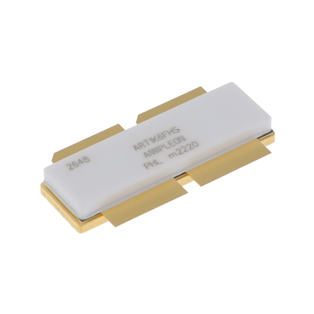
The MRF7S18125AHR3 is an N-channel enhancement-mode lateral MOSFET designed for GSM and GSM EDGE base station applications operating between 1800 MHz and 2000 MHz. It supports Class AB and Class C modulation schemes with a typical drain efficiency of 55% at 125 Watts CW output power (VDD = 28 Volts, f = 1880 MHz). The device features internal input and output matching networks to simplify circuit design. Maximum ratings include a drain-source voltage of +65 Vdc and an operating junction temperature up to 225 °C.
Verify the component status as End of Life or obsolete through official manufacturer channels before procurement planning. Confirm RoHS compliance documentation and moisture sensitivity levels. Ensure that the R3 suffix corresponds to the required tape and reel packaging specifications for your assembly line. Validate all electrical parameters against the latest datasheet revisions.
Select this component for high-power RF applications requiring integrated matching within the 1800-2000 MHz band. Consider the thermal resistance characteristics and maximum junction temperature limits for heat sink design. Evaluate the internal ESD protection requirements against system-level standards. Verify compatibility with Class AB and Class C biasing configurations for target modulation schemes.
This part belongs to the Freescale Semiconductor RF Power LDMOS transistor family, now under NXP Semiconductors. It utilizes advanced lateral MOSFET technology optimized for wireless infrastructure. The device is housed in a specific plastic package variant designed for high-power dissipation and robust performance in demanding RF environments.
Consult official manufacturer substitution lists for verified alternatives. Cross-reference pinouts and thermal characteristics carefully when evaluating potential replacements.
The typical drain efficiency is 55% when operating at VDD = 28 Volts, IDQ = 1100 mA, and Pout = 125 Watts CW at 1880 MHz.
No, the MRF7S18125AHR3 is internally matched on both the input and output ports to facilitate easier integration into amplifier designs.
The maximum operating junction temperature is specified as 225 °C.
 MRF7S18125AHR3
The activity of extra discounts on wholesale prices is in full swing…
Please fill in your contact information and we will send you the latest wholesale price list.