ChipApex | Global Electronic Components Supplier
SEARCH
Search Product
Search Post
— IC芯片 | 连接器 | 传感器 | 被动器件 —
Search productSearch post
— IC芯片 | 连接器 | 传感器 | 被动器件 —
Consult the customer manager about the wholesale price.
consultation hotline:86-132-6715-2157
email:[email protected]
Contact the product manager for consultation. One-stop consultation is available.
Do you want a lower wholesale price? Please send us your inquiry and we will reply immediately.
The MRFE6S9045NR1 is an N-Channel Enhancement-Mode Lateral MOSFET designed for broadband commercial and industrial applications up to 1000 MHz. It operates at a maximum drain-source voltage of 66 Vdc and a maximum operation voltage of 32 Vdc. The device delivers 45 W output power in GSM applications across the 920-960 MHz band with 20 dB gain and 68% efficiency. In GSM EDGE mode, it provides 16 W average output power with 20 dB gain and 46% efficiency. For single-carrier N-CDMA signals at 880 MHz, it achieves 10 W average output power with 22.1 dB gain and 32% efficiency.
Verify component authenticity through authorized distribution channels. Confirm RoHS compliance status as indicated on official documentation. Ensure proper handling procedures are followed due to moisture sensitivity level 3 classification. Validate package integrity prior to installation to maintain specified electrical characteristics.
Select this transistor for designs requiring high gain and broadband operation within the 850 to 960 MHz range. Consider the 28 Vdc operating voltage requirement and 350 mA quiescent current specifications. Evaluate thermal management needs given the 225°C junction temperature capability and plastic package constraints.
This RF power field effect transistor belongs to the Freescale Semiconductor product line, now part of NXP USA Inc. It utilizes lateral MOSFET technology specifically engineered for robust performance in demanding radio frequency environments. The component is supplied in tape and reel packaging for automated assembly processes.
Consult official manufacturer documentation for verified substitute part numbers. Cross-reference electrical parameters and physical dimensions before implementation.
The maximum operating junction temperature is rated at 225°C.
It is capable of handling 5:1 VSWR at 32 Vdc and 880 MHz with 3 dB overdrive, demonstrating enhanced ruggedness.
The typical power gain is 20 dB when delivering 16 Watts average output power across the 920-960 MHz band.
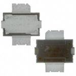 MRFE6S9045NR1
The activity of extra discounts on wholesale prices is in full swing…
Please fill in your contact information and we will send you the latest wholesale price list.