ChipApex | Global Electronic Components Supplier
SEARCH
Search Product
Search Post
— IC芯片 | 连接器 | 传感器 | 被动器件 —
Search productSearch post
— IC芯片 | 连接器 | 传感器 | 被动器件 —
Consult the customer manager about the wholesale price.
consultation hotline:86-132-6715-2157
email:[email protected]
Contact the product manager for consultation. One-stop consultation is available.
Do you want a lower wholesale price? Please send us your inquiry and we will reply immediately.
The MW6S010MR1 is a lateral N-channel enhancement-mode RF power MOSFET designed for base station applications up to 1500 MHz. It operates at 28 Vdc with a maximum drain-source voltage of 68 Vdc and total device dissipation of 61.4 W. At 960 MHz, it delivers 10 Watts PEP output power with 18 dB gain and 32% efficiency. The device supports analog/digital modulation and handles 10:1 VSWR. It features integrated ESD protection, on-chip RF feedback, and qualified operation up to 32 Vdd.
Verify the specific suffix configuration when ordering. The R1 suffix indicates tape and reel packaging containing 500 units per 24 mm reel. Confirm RoHS compliance status as the standard part has been replaced by RoHS-compliant variants. Ensure the correct package style (TO-270-2 plastic or TO-270-2 gull) matches the design requirements.
Select this component for broadband RF power amplification requiring stable operation across wide frequency ranges. The device is suitable for designs needing high linearity and robustness against load mismatches. Consider the thermal management requirements given the 61.4 W dissipation rating and the need for appropriate heatsinking to maintain junction temperature limits.
This device belongs to the Freescale Semiconductor RF Power Field Effect Transistor family. It is an N-channel enhancement-mode lateral MOSFET optimized for high-frequency power applications. The product line focuses on providing reliable solutions for communication infrastructure equipment requiring efficient signal amplification.
The MW6S010MR1 has been replaced by MW6S010NR1/GNR1. These replacements offer no form, fit, or function changes. The N suffix specifically denotes RoHS compliant versions of the original component.
The maximum operating junction temperature is 200 °C.
It is capable of handling a 10:1 VSWR at 28 Vdc, 960 MHz, and 10 Watts CW output power.
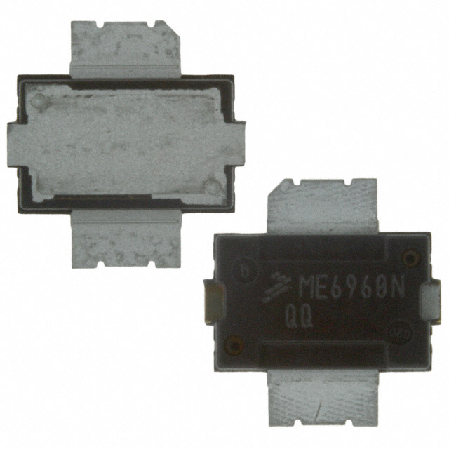
The device is available in TO-270-2 Plastic (MW6S010MR1) and TO-270-2 Gull Plastic (MW6S010GMR1).
 MW6S010MR1
The activity of extra discounts on wholesale prices is in full swing…
Please fill in your contact information and we will send you the latest wholesale price list.