 ChipApex | Global Electronic Components Supplier
SEARCH
Search Product
Search Post
— IC芯片 | 连接器 | 传感器 | 被动器件 —
Search productSearch post
— IC芯片 | 连接器 | 传感器 | 被动器件 —
Consult the customer manager about the wholesale price.
consultation hotline:86-132-6715-2157
email:[email protected]
Contact the product manager for consultation. One-stop consultation is available.
Do you want a lower wholesale price? Please send us your inquiry and we will reply immediately.
The NE68530-T1 is a surface-mount NPN silicon high-frequency transistor from the California Eastern Laboratories (CEL) NE685 series. It features a gain bandwidth product of 12 GHz and a minimum noise figure of 1.5 dB at 2.0 GHz. The device operates with a collector current of up to 30 mA, a collector-emitter voltage of 6 V, and a collector-base voltage of 9 V. Total power dissipation is rated at 150 mW in free air. The component utilizes Package Outline 30 (SOT-323 style) and includes Gummel-Poon nonlinear model parameters for circuit simulation.
Verify the specific suffix T1 against the manufacturer's current documentation to confirm availability and handling requirements. The datasheet explicitly lists the base part number NE68530 as not recommended for new designs; consult the sales office for updated design guidance or alternative recommendations before finalizing procurement specifications.
Select this component when designing circuits requiring a 12 GHz gain bandwidth product and a 1.5 dB noise figure at 2.0 GHz. Ensure the operating conditions remain within the 6 V collector-emitter voltage and 30 mA collector current limits. Consider the SOT-323 package outline for board space constraints and verify thermal derating curves if ambient temperatures exceed standard operating ranges.
This component belongs to the CEL NE685 series of high-frequency NPN silicon transistors. The series offers various package outlines including SOT-23, SOT-323, and SOT-143 styles. The NE68530 specifically corresponds to Package Outline 30. Other family members include the NE68518, NE68519, NE68533, and NE68539 variants.
The datasheet identifies the NE68530 as not recommended for new design. Verify if the NE68530-T1 is an active replacement or if the sales office recommends specific alternatives such as the NE68533 or NE68539 for new implementations.
When the stability factor K is less than or equal to 1, the Maximum Available Gain (MAG) is undefined, and Maximum Stable Gain (MSG) values are used instead.
The emitter terminal must be connected to the ground terminal of the 3-terminal capacitance bridge during measurement.
Typical noise parameters are characterized at VCE = 3 V and IC = 3 mA, though other bias points such as VCE = 1.0 V and IC = 1.0 mA are also provided in the datasheet.
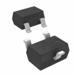 NE68530-T1
The activity of extra discounts on wholesale prices is in full swing…
Please fill in your contact information and we will send you the latest wholesale price list.







