 ChipApex | Global Electronic Components Supplier
SEARCH
Search Product
Search Post
— IC芯片 | 连接器 | 传感器 | 被动器件 —
Search productSearch post
— IC芯片 | 连接器 | 传感器 | 被动器件 —
Consult the customer manager about the wholesale price.
consultation hotline:86-132-6715-2157
email:[email protected]
Contact the product manager for consultation. One-stop consultation is available.
Do you want a lower wholesale price? Please send us your inquiry and we will reply immediately.
The NSVT5551DW1T1G is a dual NPN bipolar junction transistor array manufactured by onsemi. It integrates two independent NPN transistors within a single SOT-363 surface-mount package, designed for high-voltage applications requiring compact footprints. The device features a collector-emitter breakdown voltage of 160 V and supports a continuous collector current of 200 mA per transistor. With a maximum power dissipation of 375 mW and a DC current gain (hFE) ranging from 80 to 250 at specified test conditions, it serves as a robust solution for signal switching and amplification in space-constrained electronic designs.
Verify the manufacturer part number against official onsemi documentation to ensure authenticity. Confirm that the SOT-363 package marking matches the specific device code for the NSVT5551 series. Check for RoHS compliance status if required by your manufacturing standards. Ensure storage conditions adhere to moisture sensitivity level guidelines to prevent package damage during soldering processes.
Select this component when a design requires two isolated NPN switching elements with high voltage tolerance in a minimal footprint. Compare the 200 mA current limit against load requirements to ensure adequate headroom. Consider the thermal resistance of the SOT-363 package relative to the expected power dissipation in the final application environment.
This part belongs to the MMBT5551 family of high-voltage dual NPN transistors. It shares electrical characteristics with the single-transistor MMBT5551 but offers integrated dual-channel functionality. The 'DW' suffix indicates the SOT-363 package type, while 'T1G' denotes tape-and-reel packaging with lead-free composition.
Direct substitutes include the MMBT5551DW1T1G from onsemi or equivalent dual NPN arrays from other manufacturers offering identical 160V/200mA ratings in SOT-363 packages. Verify pinout compatibility before substitution.
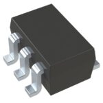 NSVT5551DW1T1G
The activity of extra discounts on wholesale prices is in full swing…
Please fill in your contact information and we will send you the latest wholesale price list.






