ChipApex | Global Electronic Components Supplier

SEARCH
Search Product
Search Post
— IC芯片 | 连接器 | 传感器 | 被动器件 —
Search productSearch post
— IC芯片 | 连接器 | 传感器 | 被动器件 —
Consult the customer manager about the wholesale price.
consultation hotline:86-132-6715-2157
email:[email protected]
Contact the product manager for consultation. One-stop consultation is available.
Do you want a lower wholesale price? Please send us your inquiry and we will reply immediately.
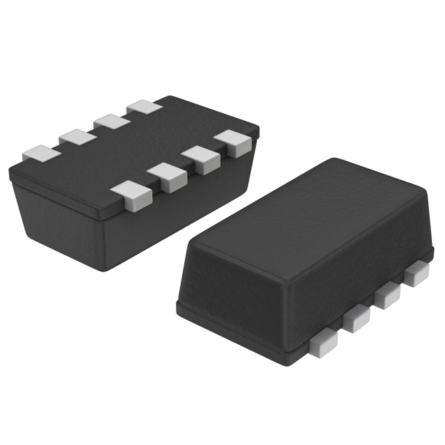
NTHD4508NT1G is listed in the FET, MOSFET Arrays range at ChipApex. The manufacturer field lists onsemi. Its product description is MOSFET 2N-CH 20V 3A CHIPFET. Review the specifications below when checking this part for your BOM.
The NTHD4508NT1G is a dual N-channel enhancement mode power MOSFET manufactured by onsemi. It features an 8-pin ChipFET package with a leadless design, offering a footprint reduction of approximately 40% compared to TSOP-6 packages. The device supports a maximum drain-source voltage (V(BR)DSS) of 20 V and a continuous drain current (ID) of 4.1 A. Typical on-resistance (RDS(on)) values are specified at 60 mΩ at VGS = 4.5 V and 80 mΩ at VGS = 2.5 V. The component operates within a temperature range of -55 °C to +150 °C junction temperature.
Verify the specific ordering suffix against official documentation to confirm packaging details. Confirm RoHS compliance status and material declarations via manufacturer sustainability resources before integration. Ensure the selected variant matches the required tape-and-reel specifications for automated assembly processes.
Select this component for low-voltage, high-current applications requiring compact board space. Evaluate thermal management requirements based on the ChipFET package's heat dissipation capabilities. Compare RDS(on) values at specific gate voltages to ensure compatibility with available drive signals in the target circuit design.
This part belongs to onsemi's Power MOSFET portfolio, specifically utilizing the ChipFET technology line. It is designed as a surface-mount solution for modern electronics where size reduction and thermal efficiency are critical. The dual-channel architecture allows for half-bridge or synchronous rectifier configurations within a minimal footprint.
Direct substitutes must match the 20 V rating, 4.1 A current capacity, and 8-pin ChipFET package dimensions. Verify that alternative components offer comparable RDS(on) values at similar gate drive voltages to maintain circuit efficiency.
The typical RDS(on) is 80 mΩ when measured at VGS = 2.5 V.
The ChipFET package offers a footprint that is approximately 40% smaller than standard TSOP-6 packages.
Yes, the component is available in a Pb-Free package compliant with RoHS standards.
Explore related parts through FETs, MOSFETs, Transistors, Discrete Semiconductor Products, all product categories.
 NTHD4508NT1G

The activity of extra discounts on wholesale prices is in full swing…
Please fill in your contact information and we will send you the latest wholesale price list.