 ChipApex | Global Electronic Components Supplier

SEARCH
Search Product
Search Post
— IC芯片 | 连接器 | 传感器 | 被动器件 —
Search productSearch post
— IC芯片 | 连接器 | 传感器 | 被动器件 —
Consult the customer manager about the wholesale price.
consultation hotline:86-132-6715-2157
email:[email protected]
Contact the product manager for consultation. One-stop consultation is available.
Do you want a lower wholesale price? Please send us your inquiry and we will reply immediately.
NTLJD3183CZTBG is listed in the FET, MOSFET Arrays range at ChipApex. The manufacturer field lists onsemi. Its product description is MOSFET N/P-CH 20V 2.6A 6WDFN. Review the specifications below when checking this part for your BOM.
The NTLJD3183CZTBG is a dual complementary power MOSFET array from onsemi, featuring an N-channel and a P-channel device integrated in a single package. It supports a maximum drain-source voltage of 20V for both channels. The N-channel configuration provides a continuous drain current of 3.2A, while the P-channel offers 2.6A. Both transistors exhibit a low on-resistance of 100mΩ. The component is housed in a compact 6-WDFN (2x2) surface-mount package.
Verify the specific suffix 'CZTBG' to ensure correct tape-and-reel packaging and RoHS compliance status. Confirm that the 6-WDFN footprint matches the target PCB design. Cross-reference the manufacturer's latest datasheet for thermal derating curves and absolute maximum ratings to prevent operational failures under high-temperature conditions.
Select this component when space-constrained designs require paired N/P-channel switching with minimal parasitic inductance. The 20V rating suits low-voltage systems. Ensure the application current remains within the 3.2A and 2.6A limits. Consider the 6-WDFN thermal performance for heat dissipation requirements compared to larger packages.
This part belongs to onsemi’s discrete semiconductor product line, specifically categorized under FET and MOSFET arrays. It serves as a compact solution for managing bidirectional or complementary power paths in portable electronics and automotive subsystems where board area is limited.
Check for direct substitutes with identical 6-WDFN pinouts and 20V/100mΩ specifications. Verify if alternative dual MOSFETs offer improved thermal resistance or higher current ratings if system margins are tight.
Explore related parts through FETs, MOSFETs, Transistors, Discrete Semiconductor Products, all product categories.
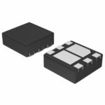 NTLJD3183CZTBG

The activity of extra discounts on wholesale prices is in full swing…
Please fill in your contact information and we will send you the latest wholesale price list.





