ChipApex | Global Electronic Components Supplier

SEARCH
Search Product
Search Post
— IC芯片 | 连接器 | 传感器 | 被动器件 —
Search productSearch post
— IC芯片 | 连接器 | 传感器 | 被动器件 —
Consult the customer manager about the wholesale price.
consultation hotline:86-132-6715-2157
email:[email protected]
Contact the product manager for consultation. One-stop consultation is available.
Do you want a lower wholesale price? Please send us your inquiry and we will reply immediately.
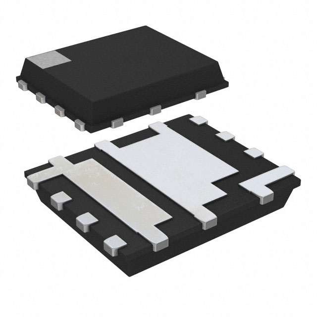
The NTMFD4C85NT3G is a PowerPhase dual N-channel MOSFET in an SO8FL (DFN8) package. It integrates a high-side FET (Q1) and a low-side FET (Q2). Q1 offers a maximum drain current of 25 A with RDS(on) of 3.0 mΩ at VGS=10V. Q2 provides 49 A with RDS(on) of 0.8 mΩ at VGS=10V. Both devices feature a 30 V breakdown voltage. The component minimizes parasitic inductances and board space requirements for synchronous buck applications.
Verify the specific ordering suffix 'T3G' corresponds to the required tape and reel quantity of 5000 units. Confirm that the DFN8 package dimensions align with the target PCB footprint. Ensure compliance with Pb-Free, Halogen Free, and RoHS standards as specified in the datasheet documentation.
Select this component for synchronous buck converters requiring compact form factors. Evaluate thermal performance based on the junction-to-ambient resistance values provided for different pad sizes. Consider gate charge characteristics for switching frequency optimization in point-of-load regulation designs.
This device belongs to the PowerPhase family of co-packaged MOSFETs from onsemi. It is designed to replace discrete high-side and low-side MOSFET pairs in DC-DC converter topologies. The integration reduces layout complexity and improves efficiency by minimizing loop inductance between the driver and the power switches.
Consult the datasheet's similar part number table for potential substitutes such as the NTMFD4C86N or NTMFD4C87N series. Verify pin compatibility and electrical parameters before substitution.
The low-side FET (Q2) has a maximum continuous drain current of 49 A under steady-state conditions at TA = 25°C.
The operating junction and storage temperature range is -55 to +150 °C.
For the high-side FET, RDS(on) increases from 3.0 mΩ at VGS=10V to 4.3 mΩ at VGS=4.5V. For the low-side FET, it increases from 0.8 mΩ at VGS=10V to 1.2 mΩ at VGS=4.5V.
 NTMFD4C85NT3G

The activity of extra discounts on wholesale prices is in full swing…
Please fill in your contact information and we will send you the latest wholesale price list.