ChipApex | Global Electronic Components Supplier

SEARCH
Search Product
Search Post
— IC芯片 | 连接器 | 传感器 | 被动器件 —
Search productSearch post
— IC芯片 | 连接器 | 传感器 | 被动器件 —
Consult the customer manager about the wholesale price.
consultation hotline:86-132-6715-2157
email:[email protected]
Contact the product manager for consultation. One-stop consultation is available.
Do you want a lower wholesale price? Please send us your inquiry and we will reply immediately.
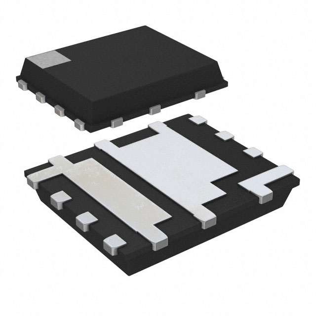
The NTMFD4C87NT1G is a PowerPhase dual N-channel MOSFET in an SO8FL (DFN8) package. It integrates a high-side FET (Q1) and a low-side FET (Q2). Q1 offers a maximum RDS(on) of 5.4 mΩ at VGS=10V and 8.1 mΩ at VGS=4.5V, with a continuous drain current of 15.4 A at 25°C. Q2 provides a maximum RDS(on) of 3.1 mΩ at VGS=10V and 4.3 mΩ at VGS=4.5V, supporting 19.5 A continuous current at 25°C. Both devices feature a 30 V drain-source breakdown voltage and operate within a junction temperature range of -55°C to +150°C.
Verify the specific ordering suffix against official documentation to confirm packaging quantity and tape-and-reel specifications. Ensure the component meets required environmental compliance standards such as RoHS and REACH before integration into final assemblies.
Select this component for applications requiring a compact dual-N-channel configuration with minimized parasitic inductance. Evaluate thermal resistance values based on the specific PCB copper area and pad size used in the design to ensure adequate heat dissipation under steady-state or pulsed conditions.
This part belongs to the PowerPhase series by onsemi, which focuses on integrated power stages. The DFN8 package (CASE 506CR) allows for efficient surface-mount assembly. The device combines two distinct N-channel MOSFETs optimized for high-side and low-side switching roles within a single footprint.
Consult official substitution guides for compatible dual N-channel MOSFETs in DFN8 packages. Verify that alternative parts match the 30 V rating, current capabilities, and thermal performance requirements of the original design.
At TA = 25°C, the high-side FET (Q1) supports 15.4 A, while the low-side FET (Q2) supports 19.5 A.
The gate threshold voltage exhibits a negative temperature coefficient, decreasing by approximately 5.0 mV/°C for Q1 and 5.1 mV/°C for Q2.
The reverse recovery charge (QRR) is typically 21 nC for Q1 and 39 nC for Q2 under specified test conditions.
 NTMFD4C87NT1G

The activity of extra discounts on wholesale prices is in full swing…
Please fill in your contact information and we will send you the latest wholesale price list.