 ChipApex | Global Electronic Components Supplier

SEARCH
Search Product
Search Post
— IC芯片 | 连接器 | 传感器 | 被动器件 —
Search productSearch post
— IC芯片 | 连接器 | 传感器 | 被动器件 —
Consult the customer manager about the wholesale price.
consultation hotline:86-132-6715-2157
email:[email protected]
Contact the product manager for consultation. One-stop consultation is available.
Do you want a lower wholesale price? Please send us your inquiry and we will reply immediately.
The NTQD6968R2 is a dual N-channel Power MOSFET from onsemi, packaged in an 8-pin TSSOP. It features a drain-to-source voltage (VDSS) of 20 Vdc and a continuous drain current (ID) of 6.6 Adc at 25°C ambient temperature. The device exhibits an ultra-low static drain-to-source on-state resistance (RDS(on)) of 22 mΩ at VGS = 4.5 Vdc and ID = 6.6 Adc. Operating within a junction temperature range of -55°C to +150°C, it incorporates logic level gate drive capability and a body-drain diode with high-speed soft recovery characteristics.
Verify the specific ordering suffix 'R2' corresponds to the Tape & Reel shipping format containing 3000 units per reel. Confirm that the component marking includes the device code '968', year code 'Y', work week 'WW', and MOSFET identifier 'N'. Ensure the procurement documentation references publication number NTQD6968/D for accurate technical specifications.
Select this component for applications requiring low conduction losses and efficient battery life extension in portable electronics. The dual channel design allows for compact board layouts using the miniature TSSOP-8 package. Verify that the 20 Vdc rating and 6.6 Adc current capacity align with the system's maximum operating conditions and thermal dissipation requirements.
This part belongs to the Power MOSFET category manufactured by onsemi. It is specifically designed as a dual N-channel enhancement mode device intended for surface mount applications. The product line emphasizes efficiency and miniaturization for use in consumer electronics and portable computing devices.
Compatible alternatives include the NTQD6968N and NTQD6968NR2. These variants share identical electrical characteristics but differ in packaging quantities or reel configurations. Verify pinout compatibility and package dimensions before substitution.
The maximum continuous drain current decreases to 4.5 Adc when the ambient temperature reaches 70°C.
The turn-on delay time is typically 9.0 ns, rise time is 35 ns, turn-off delay time is 70 ns, and fall time is 70 ns under standard test conditions.
The body-drain diode exhibits a fast reverse recovery time (trr) of typically 30 ns with a stored charge (QRR) of 0.017 μC, supporting high-speed switching applications.
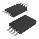 NTQD6968R2

The activity of extra discounts on wholesale prices is in full swing…
Please fill in your contact information and we will send you the latest wholesale price list.





