ChipApex | Global Electronic Components Supplier

SEARCH
Search Product
Search Post
— IC芯片 | 连接器 | 传感器 | 被动器件 —
Search productSearch post
— IC芯片 | 连接器 | 传感器 | 被动器件 —
Consult the customer manager about the wholesale price.
consultation hotline:86-132-6715-2157
email:[email protected]
Contact the product manager for consultation. One-stop consultation is available.
Do you want a lower wholesale price? Please send us your inquiry and we will reply immediately.
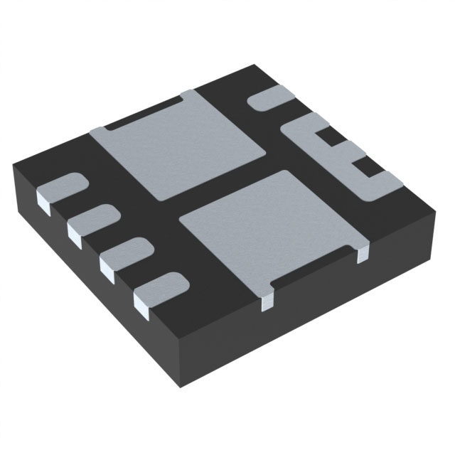
The onsemi NTTFD9D0N06HLTWG is a dual N-channel MOSFET device housed in a WQFN12 (3x3 mm) package, designated as CASE 510CJ. It integrates two dedicated N-channel MOSFETs with internally connected switching nodes to facilitate synchronous buck converter layouts. The component features a maximum drain-source voltage (VDS) of 60 V and a continuous drain current (ID) of 38 A at a case temperature of 25°C. The maximum on-resistance (rDS(on)) is specified at 9.0 mΩ when VGS = 10 V and ID = 10 A, and 13 mΩ when VGS = 4.5 V and ID = 8.0 A. The device operates within a junction temperature range of -55°C to +175°C.
Verify the specific ordering suffix TWG to confirm the reel packaging configuration and RoHS compliance status. Ensure that the procurement documentation explicitly references the WQFN12 (CASE 510CJ) physical footprint to prevent integration errors during PCB assembly. Cross-reference the manufacturer's latest datasheet revision to validate thermal resistance parameters against current design requirements.
Select this component for designs requiring a compact dual-MOSFET solution with low on-resistance for synchronous rectification. Evaluate the 9.0 mΩ rDS(on) specification at VGS = 10 V to ensure compatibility with standard gate drive voltages. Consider the 60 V breakdown voltage rating relative to input supply variations and transient spikes in the target application circuit.
This device belongs to the PowerTrench family of silicon MOSFETs from onsemi. It is part of a series of dual N-channel devices engineered specifically for high-efficiency power conversion topologies. The integration of two matched transistors in a single low-profile package reduces board space compared to discrete implementations.
Direct replacements must match the 60 V rating, dual N-channel topology, and WQFN12 footprint. Verify that alternative components offer comparable rDS(on) values at identical test conditions to maintain thermal performance.
 NTTFD9D0N06HLTWG

The activity of extra discounts on wholesale prices is in full swing…
Please fill in your contact information and we will send you the latest wholesale price list.