 ChipApex | Global Electronic Components Supplier

SEARCH
Search Product
Search Post
— IC芯片 | 连接器 | 传感器 | 被动器件 —
Search productSearch post
— IC芯片 | 连接器 | 传感器 | 被动器件 —
Consult the customer manager about the wholesale price.
consultation hotline:86-132-6715-2157
email:[email protected]
Contact the product manager for consultation. One-stop consultation is available.
Do you want a lower wholesale price? Please send us your inquiry and we will reply immediately.
The NVJD4152PT1G is a dual P-channel trench small signal MOSFET with ESD protection, manufactured by onsemi. It operates within a drain-to-source voltage range of -20 V and supports a continuous drain current of -0.88 A at 25 °C. The device features an SC-88 package (CASE 419B-02) with dimensions of 2.00 x 1.25 x 0.90 mm. Electrical characteristics include a maximum RDS(on) of 600 mΩ at VGS = -1.8 V and a total gate charge of 2.2 nC. It is qualified under AEC-Q101 standards and is PPAP capable.
Verify the specific ordering suffix 'T1G' to confirm tape and reel packaging quantities. Confirm that the NV prefix aligns with project requirements for AEC-Q101 qualification and PPAP capability. Ensure the SC-88 package style matches the PCB footprint design. Validate component authenticity through authorized distribution channels.
Select this component for space-constrained designs requiring dual P-channel isolation in an SC-88 package. Consider the -20 V rating and 0.88 A current limit for low-power switching tasks. Evaluate thermal resistance ratings against expected ambient temperatures. Compare gate charge values against driver capabilities for optimal switching speed.
This part belongs to the NTJD4152P family of dual P-channel MOSFETs. The NV prefix specifically denotes compliance with automotive quality standards and unique manufacturing site controls. It serves as a compact solution for portable electronics and automotive load switching where board space is limited.
NTJD4152PT1G
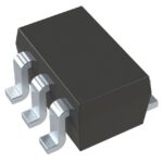 NVJD4152PT1G

The activity of extra discounts on wholesale prices is in full swing…
Please fill in your contact information and we will send you the latest wholesale price list.





