ChipApex | Global Electronic Components Supplier

SEARCH
Search Product
Search Post
— IC芯片 | 连接器 | 传感器 | 被动器件 —
Search productSearch post
— IC芯片 | 连接器 | 传感器 | 被动器件 —
Consult the customer manager about the wholesale price.
consultation hotline:86-132-6715-2157
email:[email protected]
Contact the product manager for consultation. One-stop consultation is available.
Do you want a lower wholesale price? Please send us your inquiry and we will reply immediately.
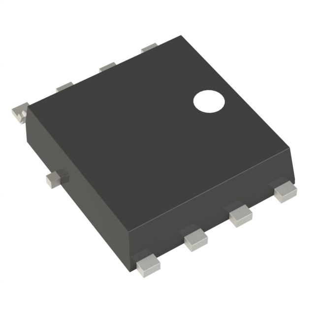
The NVMJD027N06CLTWG is a dual N-channel MOSFET from onsemi, housed in an LFPAK8 (5 x 6 mm) surface-mount package. It features a drain-to-source voltage of 60 V and a continuous drain current of 21 A at TC = 25°C. The device exhibits a low on-resistance of 27 mΩ at VGS = 10 V and 41 mΩ at VGS = 4.5 V. Total gate charge is 5 nC at VGS = 10 V and VDS = 48 V. Thermal resistance from junction to case is 6.28 °C/W. Operating temperature ranges from -55°C to +175°C.
Verify the specific ordering suffix TWG corresponds to the 3000-unit tape and reel packaging format. Confirm that the component meets RoHS compliance and lead-free manufacturing standards required by the target assembly process. Ensure the LFPAK8 thermal pad dimensions align with the printed circuit board copper pour specifications for optimal heat dissipation.
Select this component when a dual N-channel topology is necessary within strict spatial limits. Evaluate the 27 mΩ on-resistance against the maximum allowable conduction loss at the intended operating current. Verify that the 60 V breakdown voltage provides sufficient margin for the system's peak transient voltage conditions.
This part belongs to the NVMJD027N06CL series of low-voltage power MOSFETs. It utilizes silicon technology optimized for automotive applications. The LFPAK8 package provides enhanced thermal performance compared to traditional SOT packages while maintaining a small outline suitable for automated surface mount assembly processes.
Direct substitutes must match the 60 V rating, dual N-channel configuration, and LFPAK8 footprint. Verify pinout compatibility between D1/S1/G1 and D2/S2/G2 arrangements. Ensure equivalent thermal resistance and electrical parameters to maintain circuit stability without redesigning the layout or gate drive network.
 NVMJD027N06CLTWG

The activity of extra discounts on wholesale prices is in full swing…
Please fill in your contact information and we will send you the latest wholesale price list.