ChipApex | Global Electronic Components Supplier
SEARCH
Search Product
Search Post
— IC芯片 | 连接器 | 传感器 | 被动器件 —
Search productSearch post
— IC芯片 | 连接器 | 传感器 | 被动器件 —
Consult the customer manager about the wholesale price.
consultation hotline:86-132-6715-2157
email:[email protected]
Contact the product manager for consultation. One-stop consultation is available.
Do you want a lower wholesale price? Please send us your inquiry and we will reply immediately.
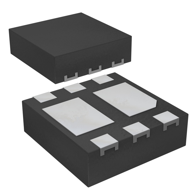
The PBSM5240PFH,115 is a hybrid module integrating a PNP low VCEsat Breakthrough In Small Signal (BISS) transistor and an N-channel Trench MOSFET within a DFN2020-6 (SOT1118) package. The BISS section supports a collector-emitter voltage of -40 V and continuous collector current of -1.8 A, with a peak current of -3 A. The MOSFET section provides a drain-source voltage of 30 V and a drain current of 0.66 A. Key electrical parameters include a typical saturation resistance of 240 mΩ for the transistor and an on-state resistance of 370 mΩ for the MOSFET at 25°C.
Verify the specific ordering suffix and tape-and-reel specifications against the manufacturer's latest documentation before finalizing procurement orders. Confirm that the component status aligns with project requirements, as product availability and manufacturing statuses are subject to change by Nexperia. Ensure compliance with RoHS directives and export control regulations applicable to your region.
Select this component when space-constrained designs require both switching and amplification functions. The integrated BISS transistor offers superior saturation performance over standard bipolar transistors. The accompanying N-channel MOSFET provides efficient switching for lower current loads. Evaluate thermal dissipation requirements based on the specific PCB copper pad area and layer configuration used in the design.
This device belongs to Nexperia's portfolio of mixed-signal modules combining bipolar and MOS technologies. It utilizes the DFN2020-6 plastic thermal-enhanced ultra-thin small outline package without leads. The marking code for this specific part number is '1T'. It is designed for surface-mount assembly using standard reflow soldering processes compatible with the specified footprint dimensions.
No public confirmed substitute part numbers are available in the provided documentation.
The maximum repetitive peak collector current (ICRM) is -2 A.
The maximum gate-source voltage (VGS) is ±8 V.
The leadless DFN2020-6 package reduces the required printed-circuit board area and allows for a lower profile compared to conventional transistor packages.
 PBSM5240PFH,115
The activity of extra discounts on wholesale prices is in full swing…
Please fill in your contact information and we will send you the latest wholesale price list.